Electronic device assembly structure

a technology of electronic devices and assembly structures, applied in the direction of electrical apparatus construction details, electrical apparatus casings/cabinets/drawers, instruments, etc., can solve the problems of unnecessary redundancy in mold making and circuit design, and achieve the effect of reducing assembly errors and damage of elements, improving usability, and saving assembly time and manpower

Inactive Publication Date: 2013-10-24
GEMTEK TECH CO LTD
View PDF9 Cites 14 Cited by
  • Summary
  • Abstract
  • Description
  • Claims
  • Application Information

AI Technical Summary

Benefits of technology

[0006]The electronic device assembly structure of the invention thus formed allows multiple sets of electronic devices to be fastened without extra accessories, hence usability improves. Assembly time and manpower of the electronic devices also can be saved. Moreover, during assembly, all the elements are visible clearly, thus assembly error and damage of the elements can be reduced.
[0007]In addition, the electronic devices and connection module of the invention adopt modular d

Problems solved by technology

Redundant mold making and ci

Method used


Image

  • Electronic device assembly structure
  • Electronic device assembly structure
  • Electronic device assembly structure

Examples


first embodiment

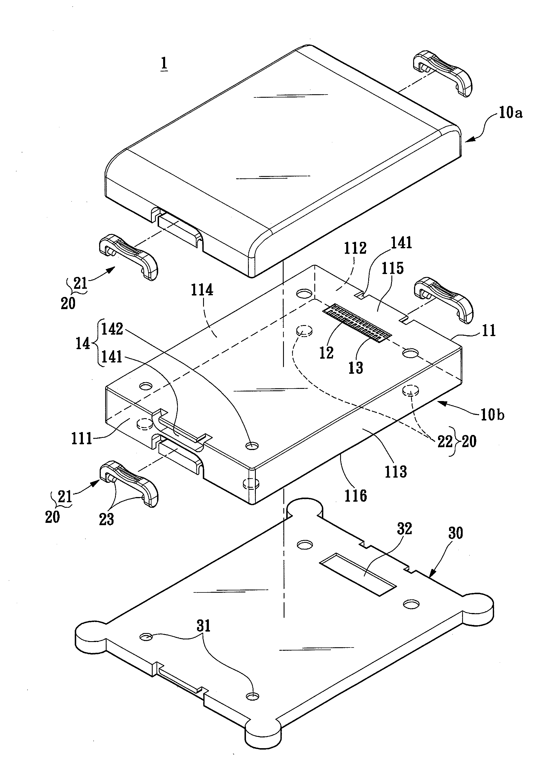
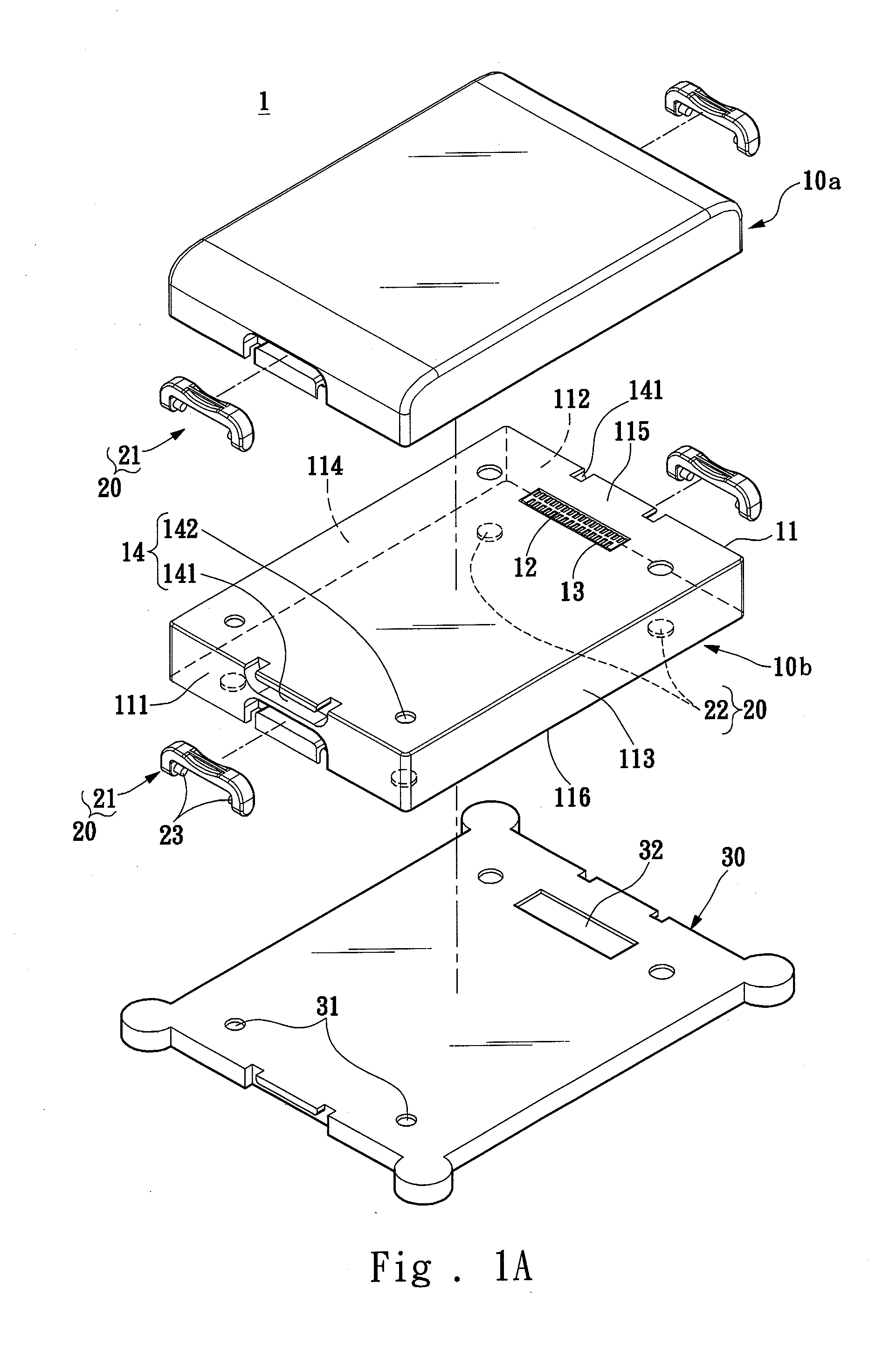
[0019]Please refer to FIG. 1A, the present invention aims to provide an electronic device assembly structure 1 that comprises at least two electronic devices 10a and 10b, and a fastening unit 20. While two electronic devices 10a and 10b are employed as an example for discussion herein, they are not the limitations of the invention.

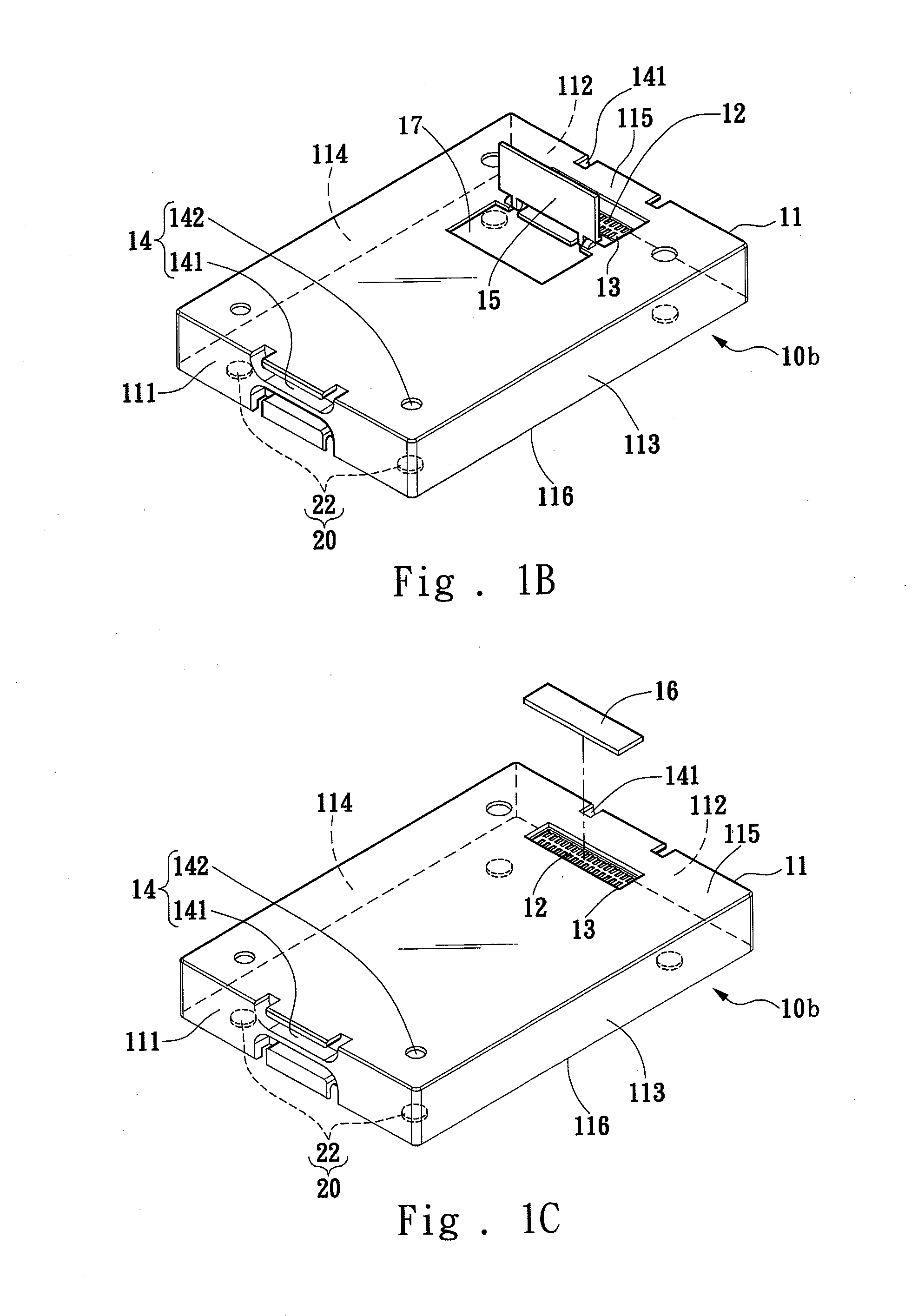
[0020]Also referring to FIG. 3, in this embodiment one electronic device 10a is stacked over another electronic device 10b. The electronic device 10b includes a body 11 and an electric connection module 12. The body 11 has at least one opening 13. The electric connection module 12 is located in the body 11. The fastening unit 20 fastens the two electronic devices 10a and 10b together in an integrated manner. The electric connection module 12 of the electronic device 10b is electrically connected to the electric connection module 12 of the electronic device 10a through the opening 13.

[0021]In this embodiment, the electronic device 10b further includes a cou...

second embodiment

[0032]Please refer to FIGS. 4, 5A and 5B for another embodiment of the electronic device assembly structure 1′ of the invention. It differs from the previous embodiment by providing a plurality of coupling slots 141′ on the coupling portion 14′ of one electronic device 10′ and a plurality of coupling arms 21′ on the fastening unit 20′.

[0033]More specifically, the coupling slots 141′ are formed on the circumference of the upper wall 111 of the body 11 in an indented manner, and the coupling arms 21′ are formed and extended from the circumference of the lower wall 112 of the body 11 corresponding to the coupling slots 141′. Each coupling slot 141′ includes a slot side wall 1411′ and a slot bottom wall 1412′. The slot side wall 1411′ has an elastic first latch structure 1413′ located thereon, and the coupling arm 21′ has an inelastic second latch structure 22′ on an outer side wall thereof. The first and second latch structures 1413′ and 22′ can be semicircular strut, but this is not t...


PUM


Abstract

An electronic device assembly structure comprises two electronic devices and a fastening unit. Each electronic device includes a body and an electric connection module. The body has at least one opening formed thereon. The electric connection module is located in the body. The fastening unit fastens the two electronic devices together in an integrated manner. The electric connection modules of the two electronic devices form electric connection through the opening.

Description

FIELD OF THE INVENTION[0001]The present invention relates to an electronic device assembly and particularly to an electronic device assembly structure equipped with modular electronic devices and electric connection modules.BACKGROUND OF THE INVENTION[0002]People living in the modern time are flooded with prolific electronic products, and among them computers are the most important ones. These days a growing number of electronic devices are linked to the computers to transmit power or data.[0003]Conventional electronic devices are formed in various shapes. When in use, it is not easy to align them neatly and connect them orderly. A lot of space also is wasted unnecessarily. Moreover, different profiles of electronic devices have to be made with different molds. Fabrication costs are higher and repairs and maintenance also are difficult.[0004]Furthermore, different electronic devices must be connected individually to a computer via multiple connection lines. This is unsightly and occ...

Claims


Application Information

Patent Timeline
IPC IPC(8): H05K7/06H05K7/00
CPCH05K7/06H05K7/005H05K5/0021H05K7/023
Inventor LIN, LUNG-HSINGCHU, CHI-CHUANYEN, CHIH-HSU
Owner GEMTEK TECH CO LTD
Why Eureka
Try Eureka