Electronic device assembly structure

a technology of electronic devices and assembly structures, applied in the direction of coupling device connections, instruments, record information storage, etc., can solve the problems of unnecessary redundancy in mold making and circuit design, and achieve the effects of reducing assembly errors and damage of elements, reducing fabrication difficulty, and saving assembly time and manpower

Active Publication Date: 2013-10-24
GEMTEK TECH CO LTD
View PDF7 Cites 19 Cited by
  • Summary
  • Abstract
  • Description
  • Claims
  • Application Information

AI Technical Summary

Benefits of technology

[0006]In short, the electronic device assembly structure of the invention can fasten a plurality of electronic devices in an integrated manner through only a connection module to save assembly time and manpower. Moreover, during assembly all the elements are visible clearly, thus can reduce assembly error and damage of the elements.
[0007]In addition, the electronic devices and connection module of the invention adopt modular design, hence can reduce fabrication difficulty and achieve product consistency. Redundant mold making and circuit design are unnecessary. Hence production cost can be greatly reduced.
[0008]Moreover, through the electronic device assembly structure of the invention, the number of electronic devices can be increased or decreased (to add or reduce the function of the electronic device assembly structure) according to user's requirements, hence can be widely used.

Problems solved by technology

Redundant mold making and circuit design are unnecessary.

Method used


Image

  • Electronic device assembly structure
  • Electronic device assembly structure
  • Electronic device assembly structure

Examples


first embodiment

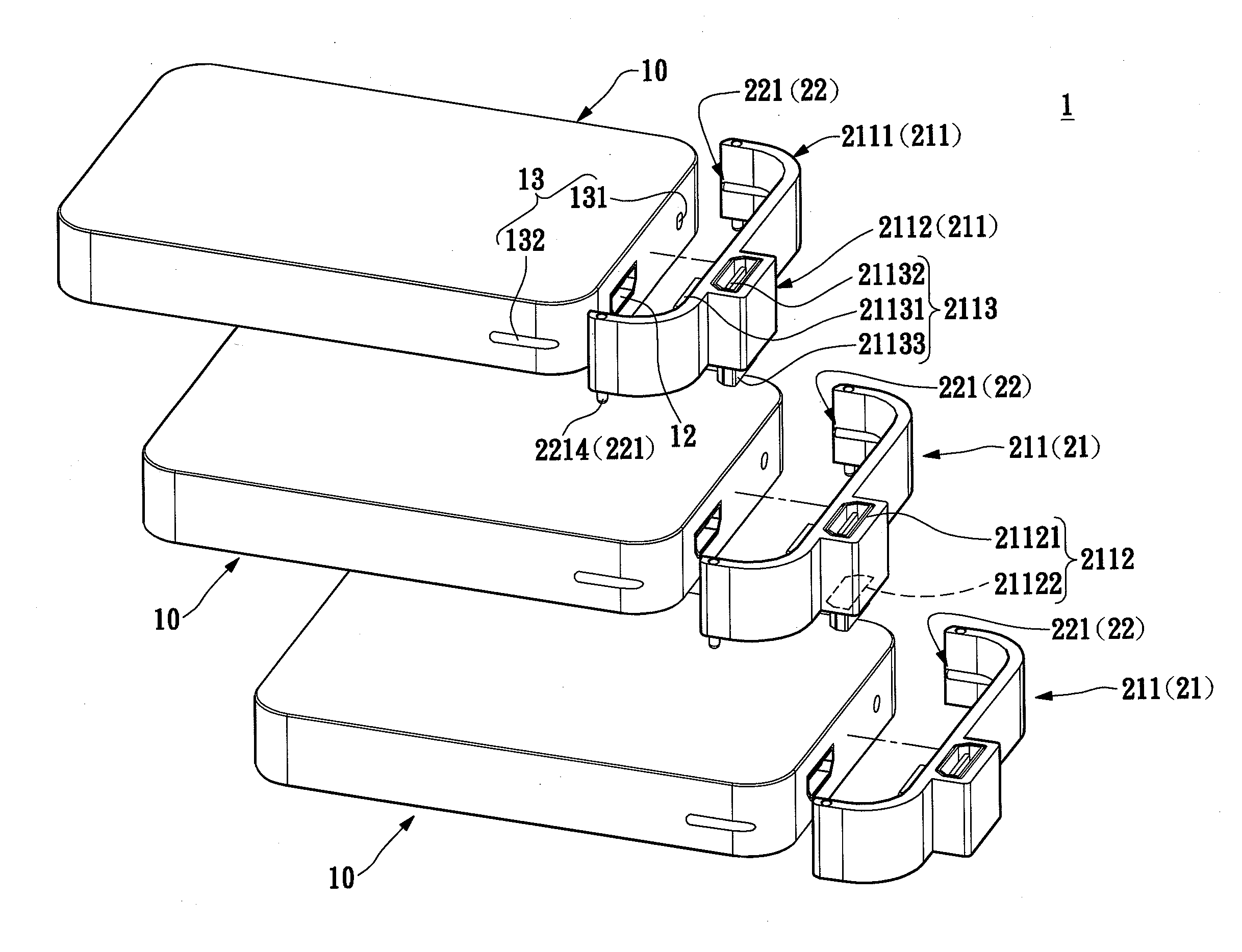
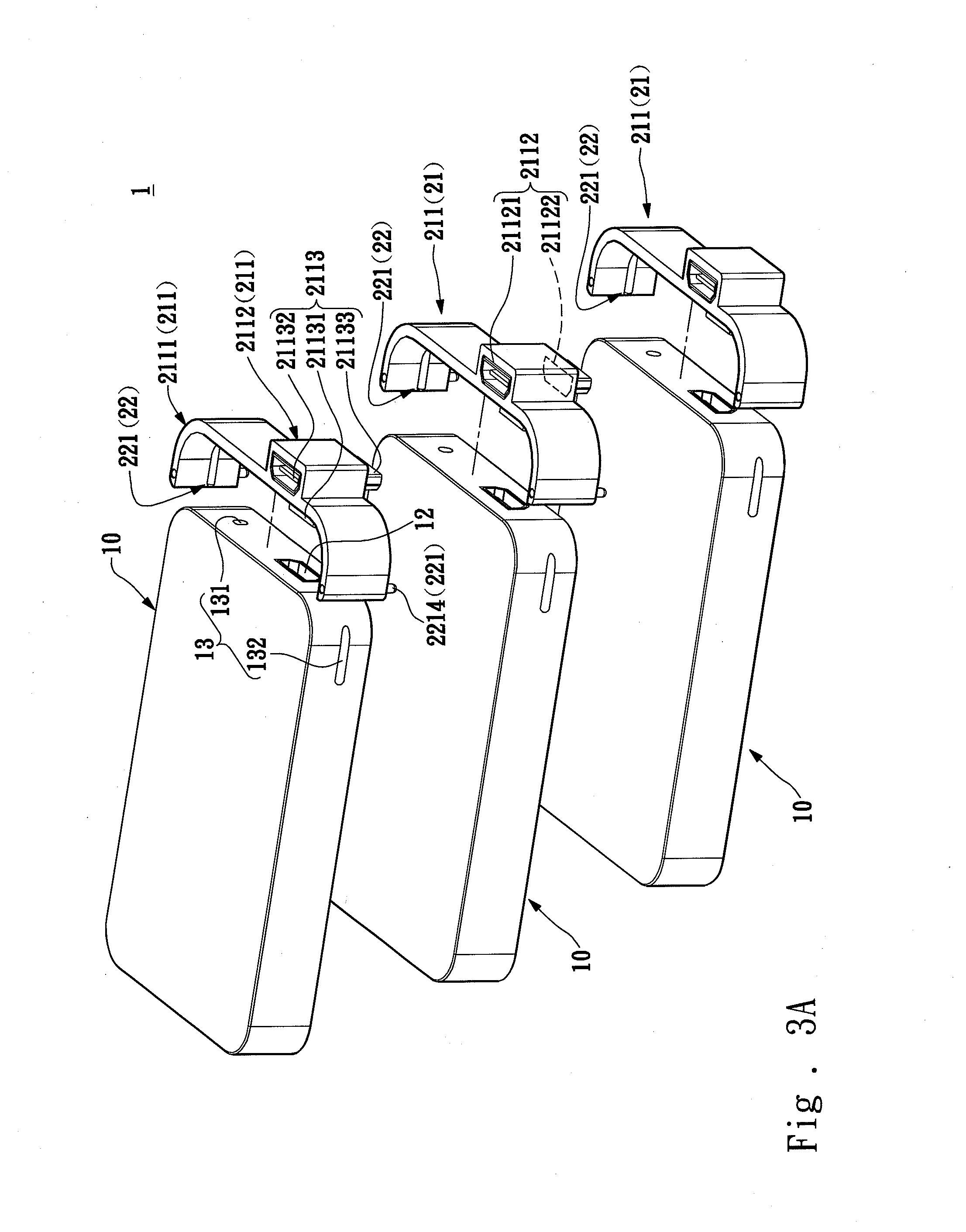
[0021]It is to be noted that in the following discussion two electronic devices 10 are taken as an example. But the actual number of the electronic devices can be adjusted according to product design requirements. Hence the discussed example shall not be deemed as the limitation of the invention.

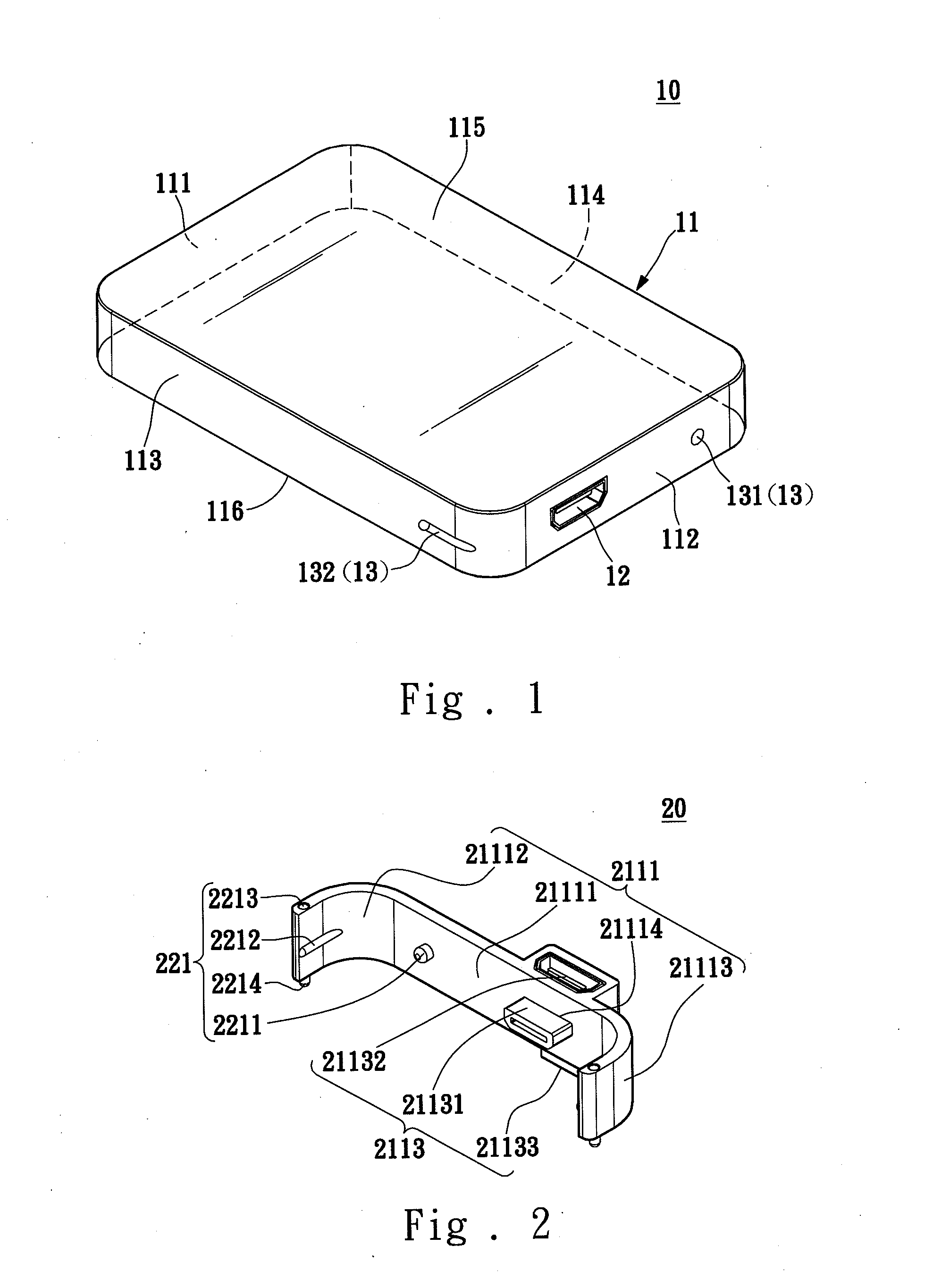
[0022]Please refer to FIGS. 1, 2, 3A and 3B for an embodiment of an electronic device assembly structure of the invention. In this embodiment one electronic device 10 is stacked over another electronic device 10. Each electronic device 10 includes a body 11 and at least one USB 12 located on the body 11. Multiple connection modules 20 can be used to fasten multiple electronic devices 10. Each connection module 20 includes an electric connection unit 21 and a fastening unit 22. The electric connection unit 21 is electrically inserted into the USBs 12 of the two electronic devices 10. The fastening unit 22 fastens the bodies 11 of the two electronic devices 10 together in an integrated manner....

second embodiment

[0032]Please refer to FIGS. 4A and 4B for another embodiment of the electronic device assembly structure 1′ of the invention. It differs from the first embodiment as follows: the coupling portion 13′ of the electronic device 10′ contains at least four latch slots 131′, and the electric connection unit 21′ includes an electric connection socket 211′, a first electric insertion socket 212′ and a second electric insertion socket 213′. The fastening unit 22′ is not located on the electric connection unit 21′, but can be an independent element.

[0033]The four latch slots 131′ are located respectively on the left wall 113 and right wall 114 of the electronic device 10′ and remote from the USB 12. The first electric insertion socket 212′ and second electric insertion socket 213′ are extended from two opposite ends of the electric connection socket 211′. The fastening unit 22′ includes at least two latch elements 221′ each including a connection arm 2211′ and latch arms 2212′ extended from t...

third embodiment

[0035]Please refer to FIGS. 5A through 5E for yet another embodiment of the electronic device assembly structure 1″ of the invention. It differs from the second embodiment as follows: the coupling portion 13″ of the electronic device 10″ includes a plurality of retaining notches 131″ for positioning and a plurality of housing notches 132″ for housing, and the fastening unit 22″ includes a plurality of lock arms 221″ and a plurality of support arms 222″.

[0036]More specifically, the retaining notches 131″ and housing notches 132″ are located on the upper wall 115 of the body 11 proximate the circumference thereof. Each lock arm 221″ is substantially formed in an L shape. The lock arms 221″ and support arms 222″ are extended from the lower wall 116 of the body 11 proximate the circumference thereof. Even more specifically, the retaining notches 131″ are located on the upper wall 115 remote from at least one USB 12. The housing notches 132″ are located on the upper wall 115 proximate th...


PUM


Abstract

An electronic device assembly structure comprises two electronic devices and at least one connection module. Each electronic device includes a body and at least one USB located on the body. The connection module connects to the two electronic devices and includes an electric connection unit and a fastening unit. The electric connection unit is electrically inserted into the USBs of the two electronic devices. The fastening unit fastens the bodies of the two electronic devices together in an integrated manner.

Description

FIELD OF THE INVENTION[0001]The present invention relates to an electronic device assembly and particularly to an electronic device assembly structure equipped with modular electronic devices and connection modules.BACKGROUND OF THE INVENTION[0002]People living in the modern time are swamped with prolific electronic products, among them computers are the most important. These days a growing number of electronic devices are linked to the computers to transmit power or data.[0003]Conventional electronic devices are formed in various shapes. When in use to align them neatly and connect them are not easy. A lot of space also is wasted unnecessarily. Moreover, different profiles of electronic devices require different molds during fabrication. Fabrication costs are higher and repairs and maintenance also are difficult.[0004]Furthermore, different electronic devices must be connected individually to a computer via multiple connection lines. This is unsightly and occupies a lot of insertio...

Claims


Application Information

Patent Timeline
Patent Type & Authority Applications(United States)
IPC IPC(8): H01R13/62
CPCH01R13/62H01R24/62H01R31/005H01R2201/06G06F1/187G11B33/025G11B33/122G06F3/00
Inventor PAI, TSUNG-HSICHAN, YUH-SHENGYEN, CHIH-HSU
Owner GEMTEK TECH CO LTD
Why Eureka
Try Eureka