Process for producing highly ordered nanopillar or nanohole structures on large areas

a nano-hole and nano-pillar technology, applied in the field of high-order nano-hole or nano-hole structure production on large areas, can solve the problems of low production cost, no products commercially available, and the use of expensive and time-consuming lithographic techniques in the order of hole arrays on the sub-150 nm rang

Inactive Publication Date: 2013-10-31
MAX PLANCK GESELLSCHAFT ZUR FOERDERUNG DER WISSENSCHAFTEN EV
View PDF8 Cites 7 Cited by
  • Summary
  • Abstract
  • Description
  • Claims
  • Application Information

AI Technical Summary

Benefits of technology

[0017]The present invention encompasses two principally different approaches to nanostructure surfaces via a cheap replication process.
[0018]A first approach involves nanoimprint lithography (NIL). In this technique a resist layer is deposited on a surface and this resist layer is then nanostructured via a stamp. Afterwards the resist is polymerized by UV-radiation or heat. Finally the stamp is removed and a thin, hardened resist layer remains on the surfaces, which can then be further processed by dry etching, sputtering or other methods. This additional step to further process the sample, is not necessary in the techniques described later in this application, but the advantage of NIL is the flexibility regarding the substrate material.

Problems solved by technology

First approaches for producing such structures concentrated on the use of expensive techniques like e-beam lithography.
These techniques lead to a decrease of the production costs to a level, which might be low enough to allow commercial launch.
However, to date there are still no products commercially available.
But almost all reports on ordered hole arrays on the sub 150 nm range still use expensive and time consuming lithographic techniques.
However, as the masters used as stamps in that technique are very expensive and have to be replaced frequently large-scale commercial use for many applications is still limited.
The use of conventional thin film antireflective coatings is difficult on optical elements made of polymers, because the adhesion of antireflective films on polymers is problematic.
However, the more important problem is, that conventional antireflective coatings would increase the production costs of the optical elements - significantly.
This is also the reason, why the technique described in Lohmüller et al. and DE 10 2007 014 538 A1 is not applicable for these very cost sensitive applications.
However, the process described in this publication is rather complicated and time consuming.
In particular it takes several days to provide a substrate nanostructured with nanopillars and the mean distance of the nanopillars is below 20 nm and cannot be adjusted easily to larger distances.
So far there is no method commercially available for the mass production of cost sensitive products with nanopillars / nanocones / nanoholes.
Nowadays commercially available tools (master stamps) for NIL are very expensive.
This prevents an easy fabrication of the master with our BCML method like described above.
Nevertheless, as production costs are a very important factor, most beamer MLAs have no antireflective coating at all.
But despite the advantages of an injection molding / hot embossing / precision molding process in comparison to directly fabricate nanostructured samples there was no cost effective method to produce molds / stamps which are decorated with ordered nanopillar arrays available until now.
As expected, it is not possible to form a closed film with sputtering only (due to the topography of the sample).

Method used


Image

  • Process for producing highly ordered nanopillar or nanohole structures on large areas
  • Process for producing highly ordered nanopillar or nanohole structures on large areas
  • Process for producing highly ordered nanopillar or nanohole structures on large areas

Examples


example 2

Preparation and Testing of a Metal Master for Injection Molding or Compress Molding Processes

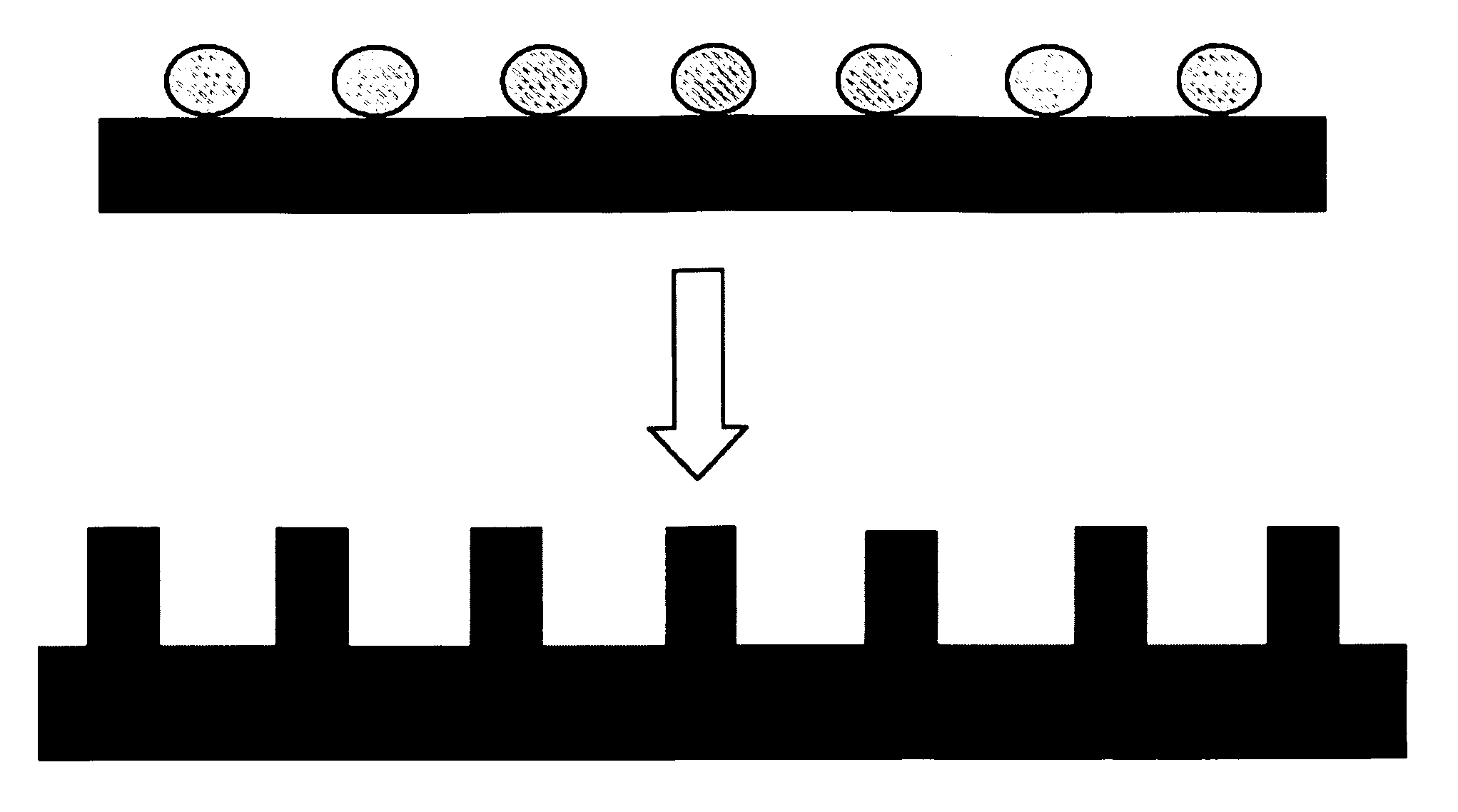
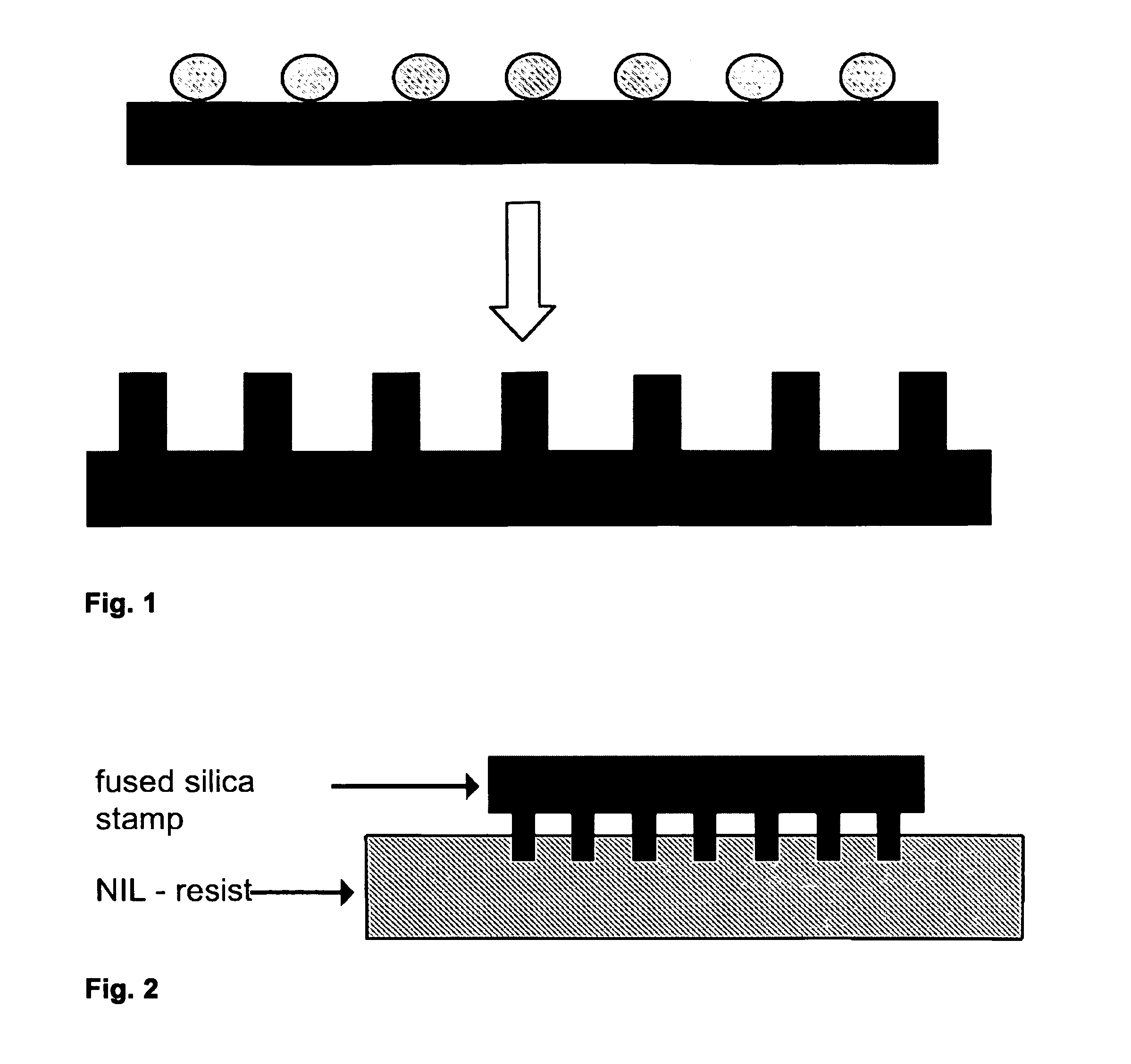
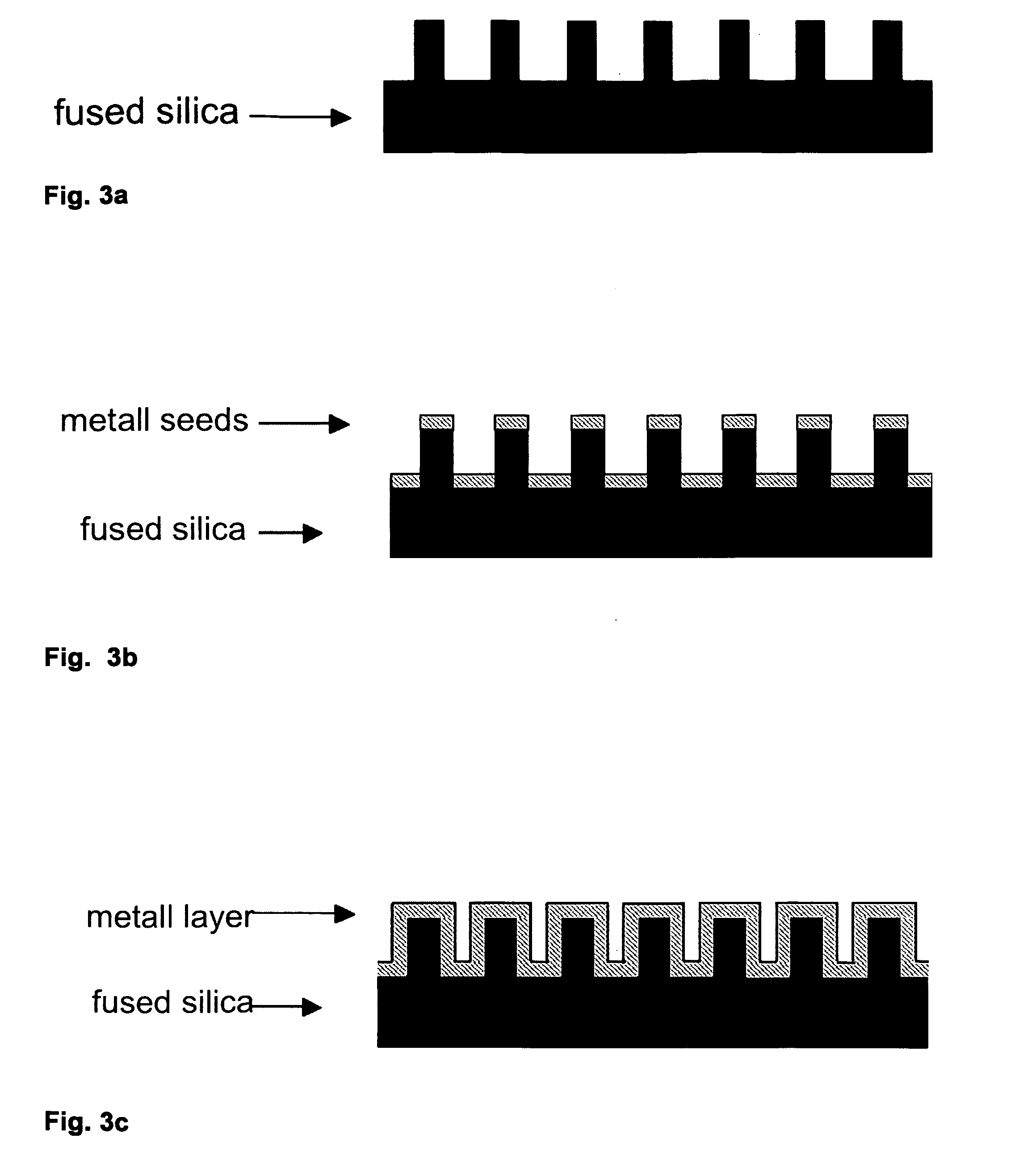
[0068]Successful fabrication of a tool for an injection molding or compress molding process was proven by the following experiments. First, a fused silica sample decorated with nanopillars or nanocones was fabricated by micellar blockcopolymer nanolithography (essentially as described in DE 10 2007 014 538 A1 or DE 10 2009 060 223.2). The resulting pillar distance was about 80 nm and pillar height about 250 nm. Subsequently, this sample has been coated with a thin gold layer of about 50 nm by sputtering (FIG. 10) for about 120 sec in a commercially available tool (Baltec MSC01). Here, gold instead of nickel or chromium was used since gold is easier to deposit via electroless deposition.

[0069]Afterwards this layer was grown further via electroless deposition (FIG. 11). For that purpose the sample has been exposed to a 1 mM solution of HAuCl4 in water. The electroless deposition has been start...


PUM

PropertyMeasurementUnit
mean distanceaaaaaaaaaa
depthaaaaaaaaaa
mean distanceaaaaaaaaaa

Abstract

The present invention relates to an improved process for producing highly ordered nanopillar or nanohole structures, in particular on large areas, which can be used as masters in NIL, hot embossing or injection molding processes. The process involves decorating a surface with an ordered array of metal nanoparticles produced by means of a micellar block- copolymer nano-lithography process; etching the primary substrate to a depth of 50 to 500 nm, where the nanoparticles act as a mask and an ordered array of nanopillars or nanocones corresponding to the positions of the nanoparticles is thus produced; using the nanostructured master or stamp in a structuring processes. Also the finished nanostructured substrate surface can be used as a sacrificial master which is coated with a continuous metal layer and the master is then etched away to leave a metal stamp having an ordered array of nanoholes which is a negative of the original array of nanopillars or nanocones.

Description

BACKGROUND OF THE INVENTION[0001]Arrays of nanopillars or nanocones on various substrate surfaces gained growing interest in recent years since they can be utilized in a broad range of important industrial applications. For example, these structures can be used as anti-reflective coatings (moth eye effect), the reduction of friction or changing the wetting properties. First approaches for producing such structures concentrated on the use of expensive techniques like e-beam lithography. Nowadays a number of bottom-up approaches have been invented which are based on self-assembly (e.g. Lohmüller, T. et al., in Nano Letters 8, 1429-1433 (2008); Park et al. in ACS Nano 3, no. 9 (2009): 2601-2608). These techniques lead to a decrease of the production costs to a level, which might be low enough to allow commercial launch. However, to date there are still no products commercially available.[0002]As already mentioned, not only the creation of nanopillar arrays is of interest, but also the ...

Claims


Application Information

Patent Timeline
Patent Type & Authority Applications(United States)
IPC IPC(8): B29C59/00
CPCB29C59/002B82Y30/00B81C99/009B81C2201/0149G03F7/0002
Inventor MORHARD, CHRISTOPHPACHOLSKI, CLAUDIASPATZ, JOACHIM P.BRUNNER, ROBERT
Owner MAX PLANCK GESELLSCHAFT ZUR FOERDERUNG DER WISSENSCHAFTEN EV
Why Eureka
Try Eureka