Scalable fabrication of one-dimensional and three-dimensional, conducting, nanostructured templates for diverse applications such as battery electrodes for next generation batteries

a nanostructure and template technology, applied in the field of ordered, nanoarrays, can solve the problems of prohibitively high cost of nanostructures, inability to realize utility of nanostructures, and inability to scale or completely reproduce the majority of methods for making such nanostructures

Inactive Publication Date: 2014-11-20
UT BATTELLE LLC
View PDF3 Cites 29 Cited by
  • Summary
  • Abstract
  • Description
  • Claims
  • Application Information

AI Technical Summary

Benefits of technology

[0009]According to certain embodiments, arrays of ordered, regularly-placed, 1D nanorods of metals / alloys can be formed by a scalable method. The 1D nanorods can be single-crystal-like when formed on a biaxially-textured substrate. Various embodiments meet the need for ordered one dimensional nanoarrays for applications such as advanced solar cell, battery architectures, electronic devices, and other applications. Various embodiments provide a scalable method for producing ordered 1D nanoarrays. Various embodiments provide a 1D nanoarray array including nanorads that are single-crystal in nature. Still other embodiments provide nanoarrays wherein all of the nanorods that make up the nanoarray have the same orientation.

Problems solved by technology

While fabrication of a variety of interesting nanostructures has been demonstrated in small samples, a predominant number of the methods for making such nanostructures are not readily scalable or completely reproducible.
Therefore, such nanostructures are prohibitively expensive and the utility thereof cannot be realized.

Method used


Image

  • Scalable fabrication of one-dimensional and three-dimensional, conducting, nanostructured templates for diverse applications such as battery electrodes for next generation batteries
  • Scalable fabrication of one-dimensional and three-dimensional, conducting, nanostructured templates for diverse applications such as battery electrodes for next generation batteries
  • Scalable fabrication of one-dimensional and three-dimensional, conducting, nanostructured templates for diverse applications such as battery electrodes for next generation batteries

Examples


Embodiment Construction

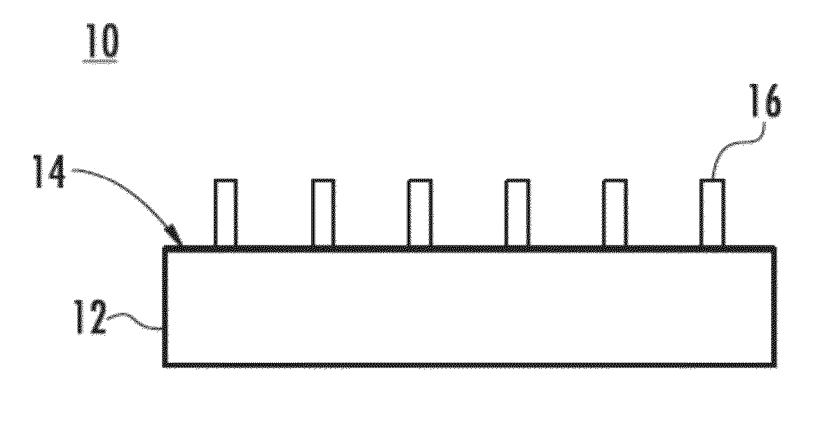
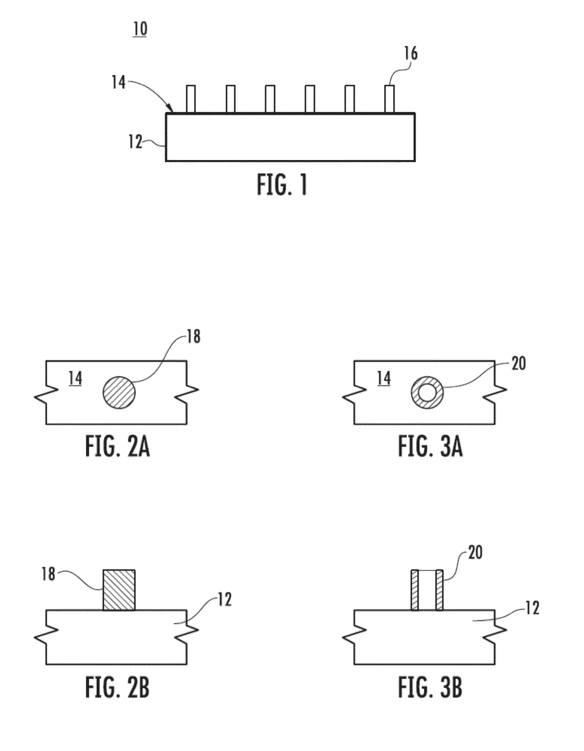
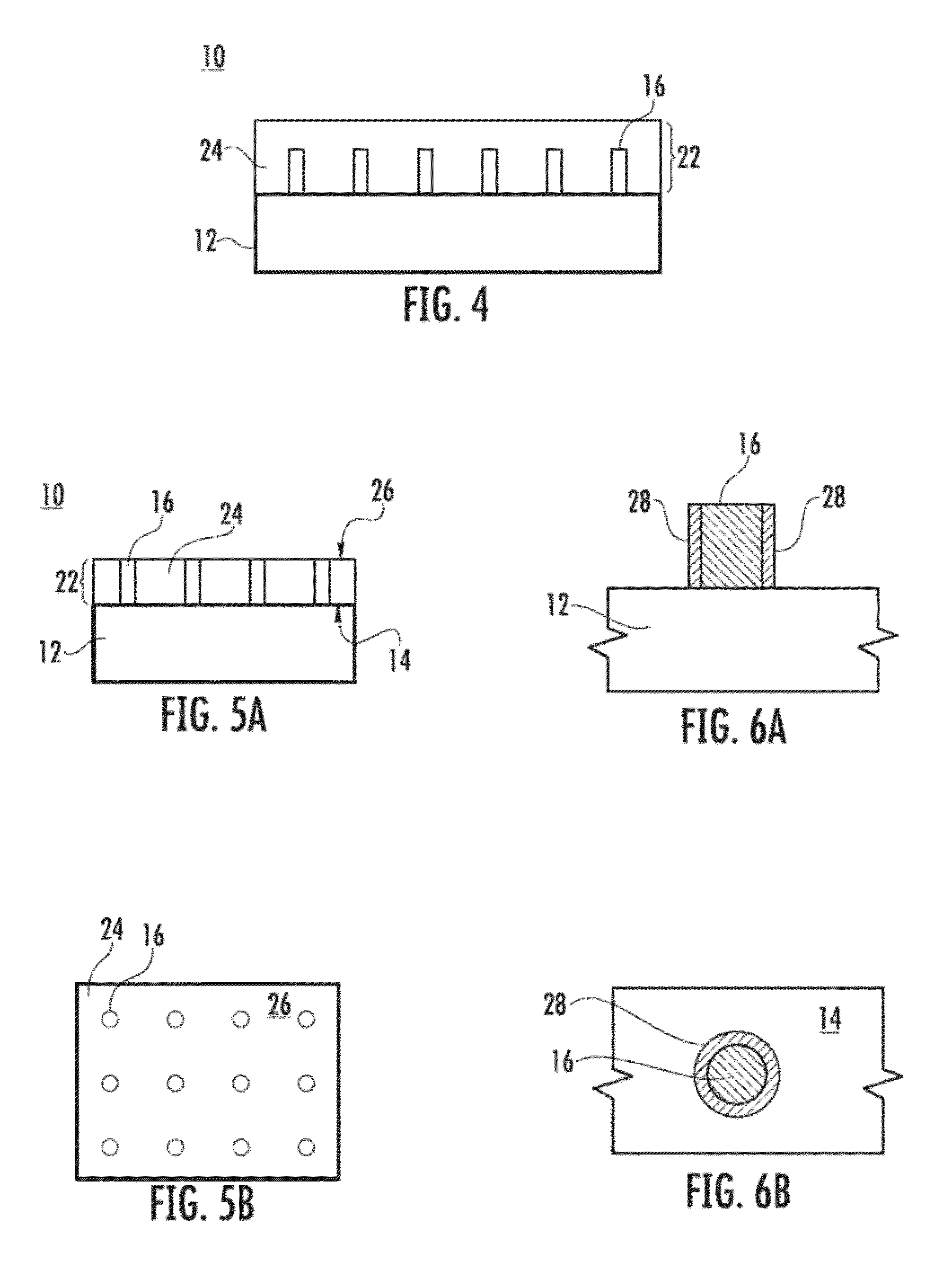
[0033]The present invention may be understood more readily by reference to the following detailed description of preferred embodiments of the invention as well as to the examples included therein. All numeric values are herein assumed to be modified by the term “about,” whether or not explicitly indicated. The term “about” generally refers to a range of numbers that one of skill in the art would consider equivalent to the recited value (i.e., having the same function or result). In many instances, the term “about” may include numbers that are rounded to the nearest significant figure.

[0034]As used herein, a first layer is “supported on” second layer if the first layer is above the second layer in a stack, whereas a first layer is “deposited on” a second layer if the first layer is above and in direct contact with the second layer. In other words, there can be intermediate layers between a first layer supported on a second layer, whereas there are no intermediate layers if the first ...


PUM

PropertyMeasurementUnit
diameteraaaaaaaaaa
diameteraaaaaaaaaa
lengthaaaaaaaaaa

Abstract

Articles including an array of one-dimensional or three-dimensional nanopillar arrays disposed on a substrate and methods for the formation thereof. The methods can include filling a plurality of hollow nanopillars, which are supported on a substrate, with a first conductive material and removing the plurality of hollow nanopillars to leave a plurality of vertically-aligned, epitaxial nanopillars, comprising the first conductive material, on the substrate.

Description

CROSS-REFERENCES TO RELATED APPLICATIONS[0001]This application is a Continuation-in-Part of U.S. patent application Ser. No. 12 / 849,970, filed Aug. 4, 2010, titled Vertically-Aligned Nanopillar Array on Flexible, Biaxially-Textured Substrates for Nanoelectronics and Energy Conversion Applications, which claimed priority to U.S. Provisional Application No. 61 / 231,501, filed Aug. 5, 2009, claimed priority to U.S. Provisional Application No. 61 / 231,063, filed Aug. 4, 2009, and was a continuation-in-part of U.S. application Ser. No. 12 / 711,309, entitled “Structures with Three Dimensional Nanofences Comprising Single Crystal Segments,” filed Feb. 24, 2010, the entireties of which are incorporated herein by reference.STATEMENT REGARDING FEDERALLY SPONSORED RESEARCH OR DEVELOPMENT[0002]The United States Government has rights in this invention pursuant to contract no. DE-AC05-00OR22725 between the United States Department of Energy and UT-Battelle, LLC.BACKGROUND OF THE INVENTION[0003]1. Fi...

Claims


Application Information

Patent Timeline
Patent Type & Authority Applications(United States)
IPC IPC(8): H01M4/78H01M4/04
CPCH01M4/0402H01M4/78B82Y10/00C25D5/02C25D7/00C25D11/045G11B5/746G11B5/82G11B5/855H01L29/0676B82Y40/00H01L29/66439H01L29/66469H01L29/775C30B29/02C30B29/605C25D1/003C25D11/20C25D11/26B81C1/00031H01M4/1395H01M4/386H01M4/661B32B15/02B32B15/043B32B15/20B32B2260/046Y02E60/10
Inventor GOYAL, AMIT
Owner UT BATTELLE LLC
Why Eureka
Try Eureka