Interconnect structures with engineered dielectrics with nanocolumnar porosity

a technology of nanocolumnar porosity and interconnect structure, which is applied in the manufacture of multilayer circuits, semiconductor devices, semiconductor/solid-state device details, etc., can solve the problems of fracture toughness and cohesive strength, the effective dielectric constant of the interconnect structure is reduced, and the overall speed of the operation of these advanced chips is beginning to be limited.

Active Publication Date: 2005-04-14
GLOBALFOUNDRIES US INC
View PDF3 Cites 24 Cited by
  • Summary
  • Abstract
  • Description
  • Claims
  • Application Information

AI Technical Summary

Benefits of technology

[0024] The interconnect structure of the present invention used for the purposes set forth above embodies a first dielectric material encasing a set of conductive vias and supporting thereon a set of conductive lines on its top surface. There is, in addition, a second dielectric disposed between the set of conducting lines and possessing a top surface and a bottom surface. The second dielectric contains a regular array of nanocolumnar pores which are sealed off at the top by a layer of a third dielectric layer which serves to protect the top surface of the conductive lines. Specific copolymers are used as templates or stencils to obtain the “regular array” in accordance with the present invention. The expression “regular array” is used herein to designate an ordered arrangement of separated phases, such as in a hexagonal closed pack pattern. For the purpose of this disclosure, “nanocolumnar” describes a structure generated from the regular array noted above, which is transferred anisotropically into an underlying material stack which can include one or more of the layers selected from the group comprising: hardmask, cmp stop, etch stop, line-level dielectric and via level dielectric. The invention generally relates to generating nanocolumnar voids or nanocolumnar pillars in a dielectric stack in order to reduce the effective dielectric constant of the interconnect structure.

Problems solved by technology

With the progress in the transistor device technology leading to the present ultra large scale integration, the overall speed of operation of these advanced chips are beginning to be limited by the signal propagation delay in the interconnection wires between the individual devices on the chips.
Although a tunable range of k values is possible with this set of very low k materials, there are several difficulties in integrating these materials with copper interconnects by the dual damascene process described above.
These low k dielectrics have a much lower elastic modulus, fracture toughness and cohesive strength than the silicon dioxide or FSG films and their adhesion to typical hard mask layers used in current state of the art copper interconnect is also correspondingly inferior.
This renders the DD process highly impractical from the point of view of manufacturability and yields.
There are other issues associated with integrating very low k porous dielectrics with interconnected porosity that pertain to the metallization and plating of wiring layers.
This in turn can lead to line to line shorting.
Poor coverage of the rough surfaces of the porous dielectric surfaces by these barriers can also lead to infiltration of the plating and cleaning solutions into the dielectric.
Poor coverage can also lead to Cu diffusion into the dielectric during subsequent thermal processing cycles which can cause a degradation in the electrical breakdown behavior of the intermetal dielectric (IMD).
These requirements are often conflicting in nature and are restrictive of the extent of porosity that can be generated and hence the lowering of the dielectric constant of the IMD.
Such a porous structure is generally weaker in mechanical strength and sometimes exhibits spatial variability in the dielectric properties as a result of the pore size distribution.
While this prior art method does avoid all the issues associated the direct DD integration of the porous IMDs, it requires that the porous IMD be able to fill line to line gaps and withstand CMP planarization which can restrict the choices of the porous IMD.
Further, additional process steps to etch the support dielectric and fill and polish the gapfill porous dielectric are needed which can add to manufacturing cost and lead to possible reduction in yield.

Method used


Image

  • Interconnect structures with engineered dielectrics with nanocolumnar porosity
  • Interconnect structures with engineered dielectrics with nanocolumnar porosity
  • Interconnect structures with engineered dielectrics with nanocolumnar porosity

Examples


first embodiment

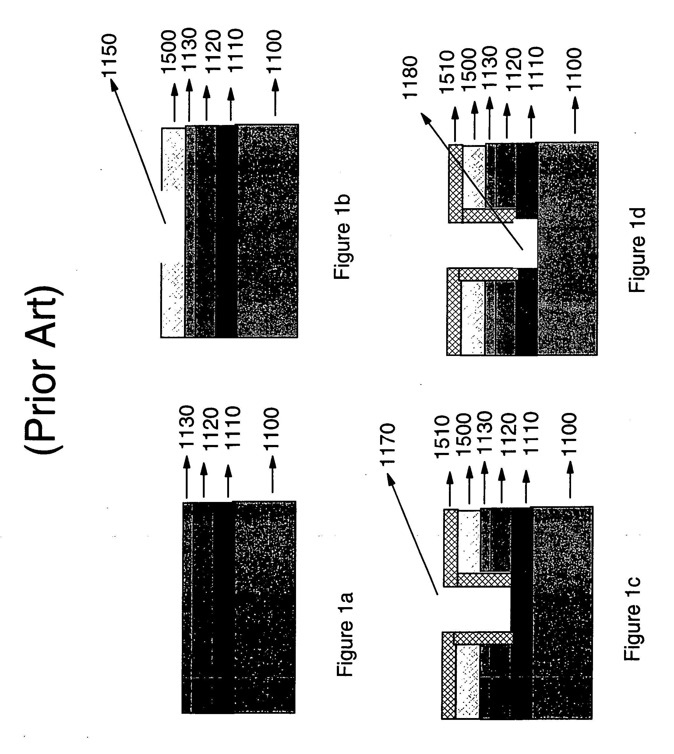
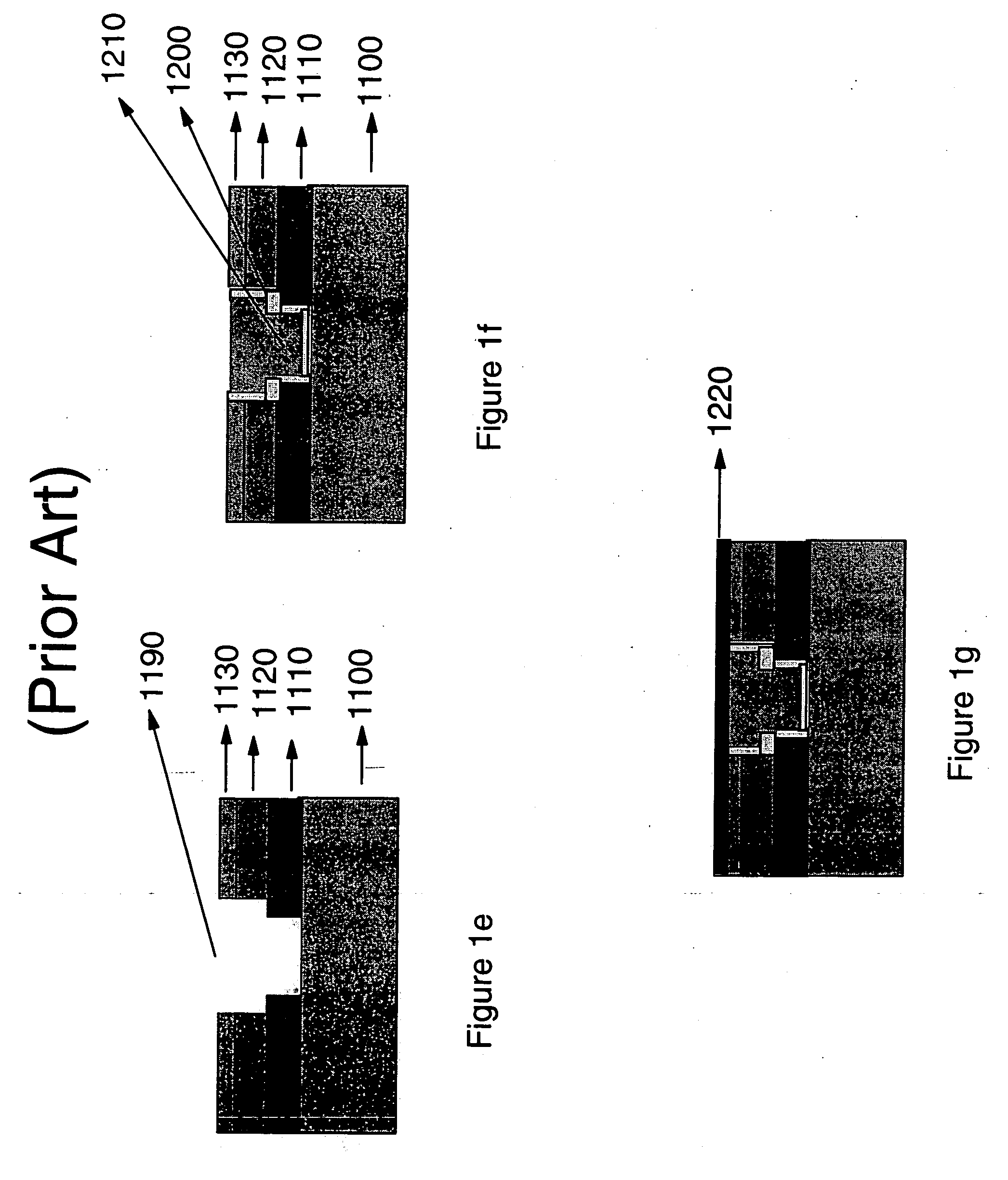
[0031] The method of the first embodiment begins with the fabrication of a dual damascene interconnect structure comprising the prior art steps described earlier and depicted in the steps FIG. 1a through FIG. 1f resulting in embedded Cu lines coplanar with the IMD surface. The DD structure is built using IMD materials, which are preferably more robust compared with the very low k dielectrics described in the prior art. Such a robust IMD material can be selected from, but not restricted to, the set comprising (a) organic thermoset dielectrics such as polyarylene ethers (for example SiLK™ produced by Dow Chemical Company or GX3™ produced by Honeywell Microelectronic Materials) (b) spun on silica or organosilicate glass films, (c) hydrogenated amorphous dilectrics comprising Si, C, H and O and deposited by plasma enhanced chemical vapor deposition (PECVD), (d) undoped silicon oxide glass (USG) and fluorine doped silicon oxide glass (FSG) deposited by PECVD, (e) porous versions of (a)-(...

embodiment 2

[0044] In another embodiment (embodiment 2) of this inventive method, illustrated in FIG. 3, the following sequence of steps is additionally performed after the holes 2160 (and holes 2170 and 2180 by analogy) are formed into the IMD and the diblock polymer layer has been etched away.

[0045] An additional RIE step is performed to etch and recess the IMD layer 1130 and optionally a small depth into layer 1120 so that the etched surface is recessed below the surface of the conductive fill 1210 in the structure as shown in FIG. 3a. This recess 3000 is chosen to be about 10 nm to 60 nm but preferably about 20 nm.

[0046] The pinch off dielectric cap 2170 is then deposited such that it pinches off the holes 2160 in the recessed region created above, and covers over the surface of conductive fill 1210.

[0047] An optional CMP step can be employed to planarize the surface of dielectric cap 2170. The net result of this sequence of steps is to provide a non perforated dielectric region 2171 in g...

third embodiment

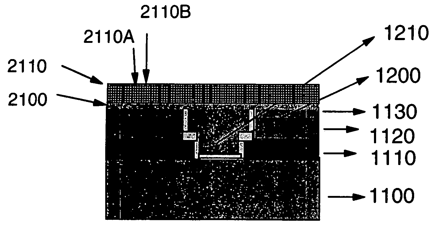
[0049] In the present inventive method, the nanocolumnar diblock stencil film 2110 is generated as described earlier in reference to FIG. 2, except that the structure is generated on a cap layer dielectric 1220 formed on top of the state of the art interconnect structure as exemplified in FIG. 1g. This is shown schematically in FIG. 4a. The remaining matrix 2140 of the stencil is used to transfer the pattern into the cap dielectric layer 1220 resulting in a perforated cap layer dielectric 4000 which rests on the top IMD layer 1130. This transfer process is performed by reactive ion etching. The nanoscale pattern in the perforated cap layer dielectric is then transferred into the IMD stack using the matrix 2140 and patterned cap layer dielectric 4000 as a mask as shown in FIG. 4b. The nanoscale pattern is transferred into the IMD stack 1110, 1120, 1130 generating columnar holes 4010. Analogous structures to those in FIGS. 2f and 2g can also be generated by adjusting the depth of the ...


PUM


Abstract

A method for forming an interconnect structure with nanocolumnar intermetal dielectric is described involving the construction of an interconnect structure using a solid dielectric, and introducing a regular array of vertically aligned nanoscale pores through stencil formation and etching to form a hole array and subsequently pinching off the tops of the hole array with a cap dielectric. Variations of the method and means to construct a multilevel nanocolumnar interconnect structure are also described.

Description

BACKGROUND OF THE INVENTION [0001] 1. Technical Field of the Invention [0002] The present invention relates generally to very high performance microelectronic chips used in computers, microprocessors, microcontrollers, sensors, communication devices and the like. In particular, the invention relates to the interconnect wiring networks on such chips, with the goal of significantly reducing the signal propagation delay associated with these wires in the networks using copper wiring embedded in a very low k dielectric medium possessing engineered porosity formed after the interconnects are formed. [0003] 2. Description of the Background Art [0004] High performance microprocessor, microcontroller and communication chips require very high speed interconnects between the active transistor devices which are used to perform the various functions such as logical operations, storing and retrieving data, providing control signals and the like. With the progress in the transistor device technol...

Claims


Application Information

Patent Timeline
Patent Type & Authority Applications(United States)
IPC IPC(8): H01L21/311H01L21/60H01L21/768H01L23/52H05K3/10H05K3/46
CPCH01L21/31144H01L21/7682H01L2924/0002H01L2924/00
Inventor COLBURN, MATTHEW E.NITTA, SATYA V.PURUSHOTHAMAN, SAMPATHBLACK, CHARLESGUARINI, KATHRYN
Owner GLOBALFOUNDRIES US INC
Why Eureka
Try Eureka