Electric interconnecting structure on substrate and producing method thereof

A technology of electrical interconnection and interconnection, applied in the direction of circuits, electrical components, electrical solid devices, etc., can solve the problem of increasing the effective dielectric constant

Inactive Publication Date: 2007-04-04
GLOBALFOUNDRIES INC
View PDF10 Cites 2 Cited by
  • Summary
  • Abstract
  • Description
  • Claims
  • Application Information

AI Technical Summary

Problems solved by technology

Therefore, higher permittivity materials (typically SiC with k=4.1) must remain in the structure, resulting in an increase in the effective permittivity

Method used


Image

  • Electric interconnecting structure on substrate and producing method thereof
  • Electric interconnecting structure on substrate and producing method thereof
  • Electric interconnecting structure on substrate and producing method thereof

Examples


example

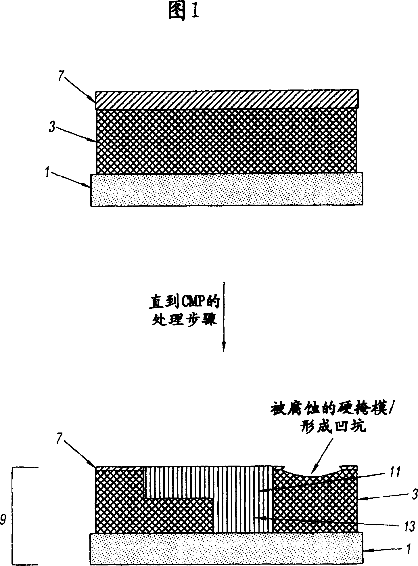
[0080] A fabricated SiLK TM / HOSP BEST TM / BLOk TM structure

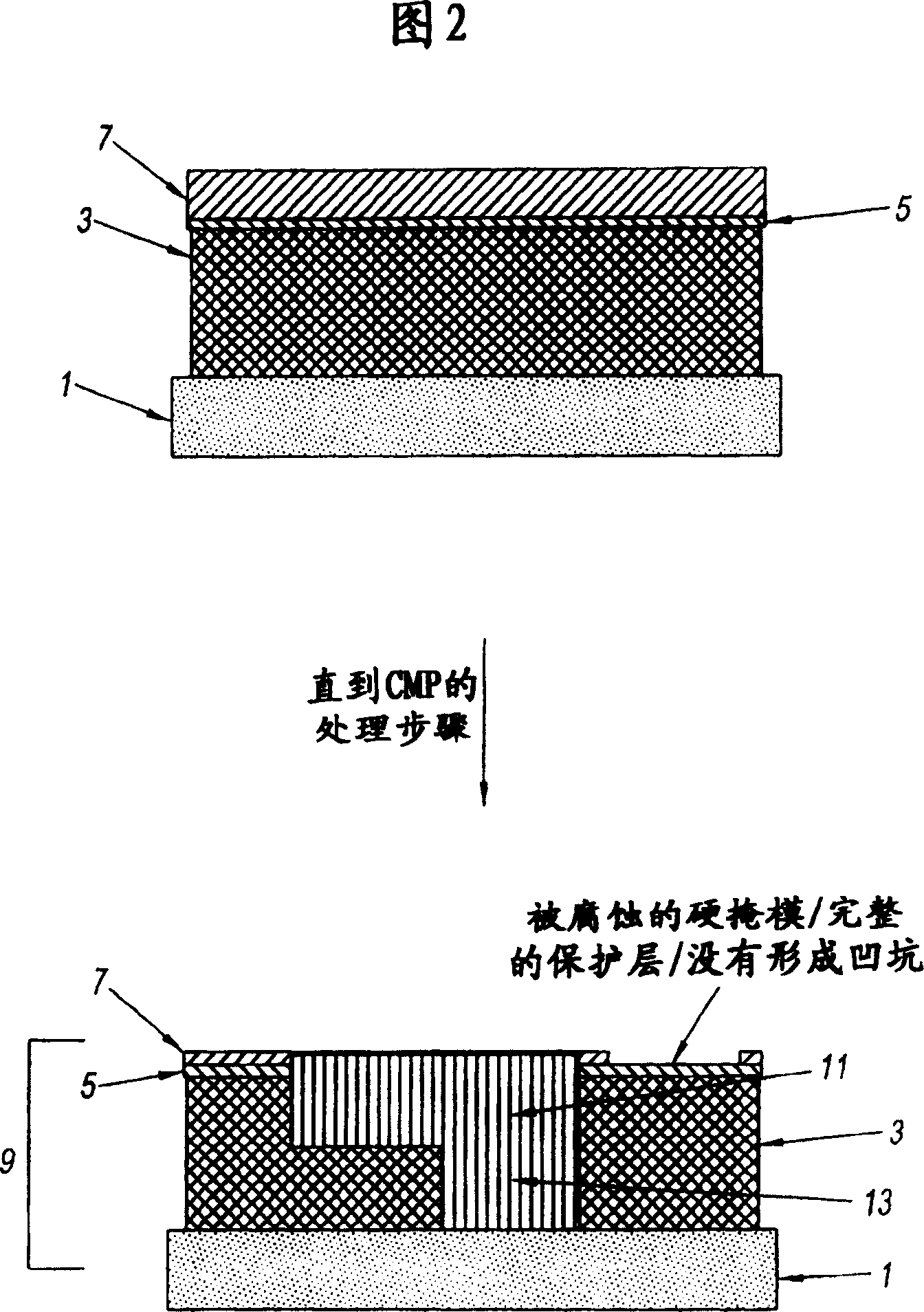
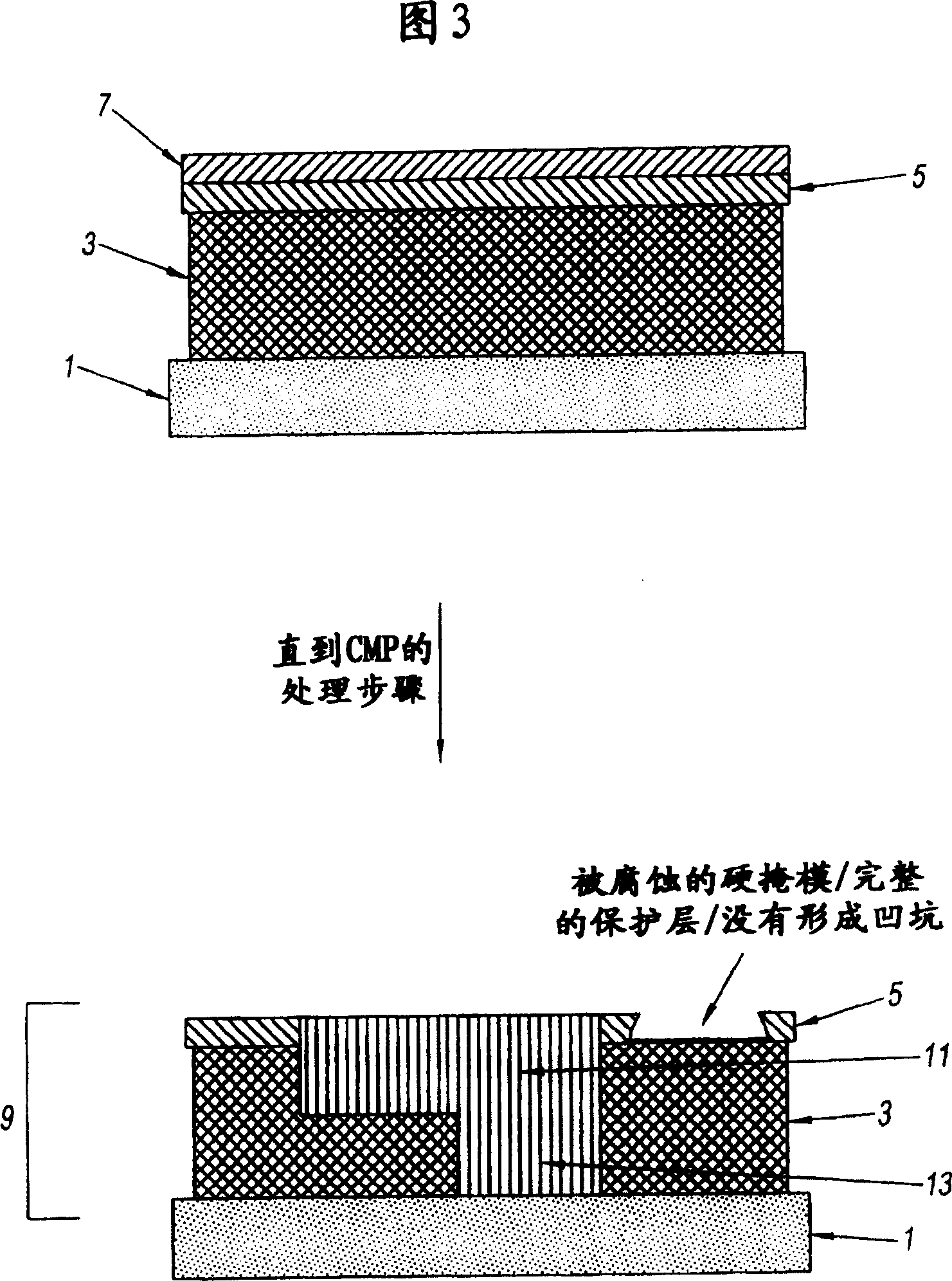
[0081] A. Lamination of dielectric layers as shown in Figure 2

[0082] steps

condition

spin coating

adhesion promoter

hot plate baking

310℃ / 90s

spin coating

First ILD layer (SiLK)

hot plate baking

310℃ / 2min.

spin coating

CMP protection layer (HOSP BESt)

hot plate baking

310℃ / 2min

to bake

Furnace -415℃ / 60min.

CVD deposition

Silicon carbide

[0083] See Table I and Figure 2 above, by adding the AP 6000 TM A 200 mm diameter silicon wafer was treated with the adhesion promoter by coating the solution onto the wafer and then spinning at 3000 rpm for 30 seconds. At 22, the wafer was then placed on a hot plate at 310° C. for 120 seconds for a first hot plate bake.

[0084] After cooling the wafer to room temperature, the first layer of low-k dielectric (SiLK TM ) (Figure 2, layer 3). SiLK TM The solution w...


PUM


Abstract

An electrical interconnect structure on a substrate, which includes: a first low-k dielectric layer; a spin-on low k CMP protective layer that is covalently bonded to the first low-k dielectric layer; and a CVD deposited hardmask/CMP polish stop layer is provided. Electrical vias and lines can be formed in the first low k dielectric layer. The spin-on low k CMP protective layer prevents damage to the low k dielectric which can be created due to non-uniformity in the CMP process from center to edge or in areas of varying metal density. The thickness of the low-k CMP protective layer can be adjusted to accommodate larger variations in the CMP process without significantly impacting the effective dielectric constant of the structure.

Description

technical field [0001] This invention relates to interconnect structures for high speed microprocessors, application specific integrated circuits (ASICs) and high speed IC's. More specifically, the present invention provides low or ultra-low dielectric constant (k) interconnect structures that increase circuit speed, accurate value of conductor resistance, and improve mechanical integrity. Background technique [0002] Many dual damascene low-k dielectric plus Cu interconnect structures are known. Such as dual damascene process, where SiLK TM For use as a low-k dielectric material, see US Patent 6,383,920, assigned to the same assignee as the present invention and incorporated by reference in its entirety as if fully set forth herein. [0003] The integration of low and ultra-low dielectric constant (k) materials requires a chemical mechanical planarization (CMP) polish stop layer in order to protect the underlying dielectric and prevent corrosion and dishing of low-k diel...

Claims


Application Information

Patent Timeline
Patent Type & Authority Patents(China)
IPC IPC(8): H01L23/52H01L21/31H01L21/312H01L21/4763H01L21/3205H01L21/768H01L21/283H01L21/304H01L23/522H01L23/532
CPCH01L2924/0002H01L23/5329H01L21/76829H01L21/76832H01L21/7688H01L21/76828Y10T428/31663H01L21/7684H01L21/76807H01L2924/00H01L21/283H01L21/304H01L21/31
Inventor 李·M·尼科尔森曾伟志克里斯蒂·泰博格
Owner GLOBALFOUNDRIES INC
Why Eureka
Try Eureka