Double-grid vertical channel field effect transistor and its manufacturing method

A technology of transistors and dojos, applied in semiconductor/solid-state device manufacturing, semiconductor devices, electrical components, etc., can solve the problems of poor quality of single crystal silicon, large leakage current of devices, and inability to realize dual-gate vertical channel devices, etc. The effect of suppressing the short-channel effect of the device, reducing the leakage current, and high integration

Inactive Publication Date: 2009-03-11
PEKING UNIV +1
View PDF4 Cites 0 Cited by
  • Summary
  • Abstract
  • Description
  • Claims
  • Application Information

AI Technical Summary

Problems solved by technology

This structure uses replacement gate technology and amorphous silicon recrystallization to form a channel technology to realize a vertical channel device with a fully depleted ultra-thin channel with a channel length of 50nm; but this method can only achieve full consumption of a single gate. As far as the vertical channel device is concerned, the quality of single crystal silicon in the channel region formed by the recrystallization of amorphous silicon is not good, and the leakage current of the device is large
[0007] None of the above three structures and their preparation methods can achieve an ideal double-gate vertical channel device.

Method used


Image

  • Double-grid vertical channel field effect transistor and its manufacturing method
  • Double-grid vertical channel field effect transistor and its manufacturing method
  • Double-grid vertical channel field effect transistor and its manufacturing method

Examples


Embodiment Construction

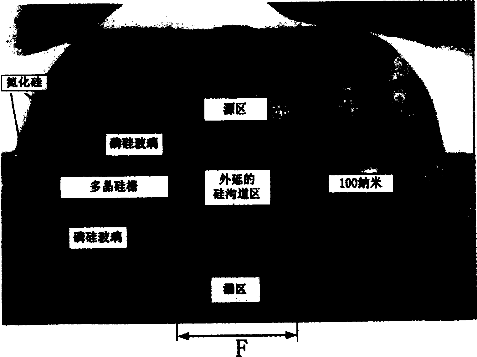
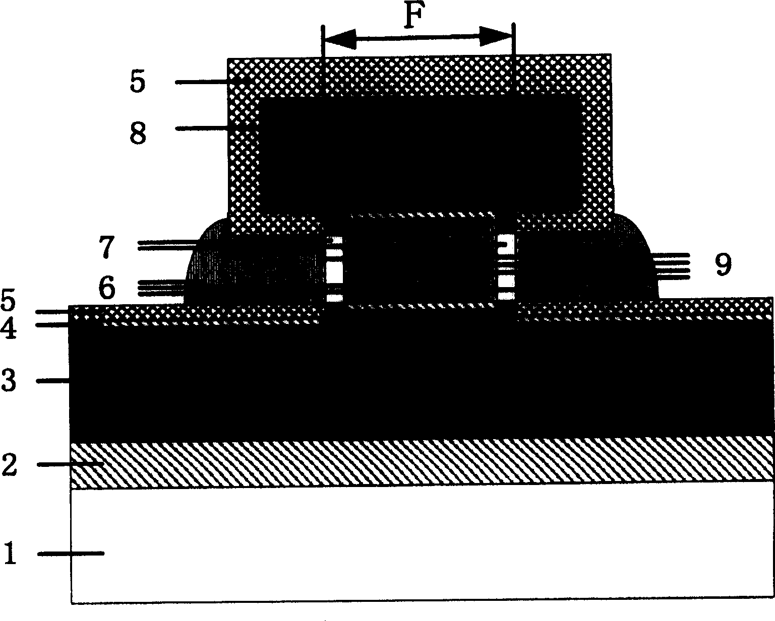
[0024] Such as figure 2 As shown, it is a schematic cross-sectional structure diagram of a specific embodiment of the novel fully depleted double-gate vertical channel field-effect transistor of the present invention. ) 3, buffer silicon dioxide 4, deposited silicon nitride 5, polysilicon germanium gate 6, vertical channel 7, polysilicon drain region (n+ doped) 8 and gate oxide layer 9. The channel length of the device is 50 nanometers (that is, the thickness of the silicon dioxide replacement gate layer is 50 nanometers), the thickness of the channel region is 20 nanometers (that is, the thickness of the polycrystalline germanium sacrificial layer is 20 nanometers), and the thickness of the gate oxide layer is 1.5 nanometers, using a 248-nanometer (optical lithography feature size F) process.

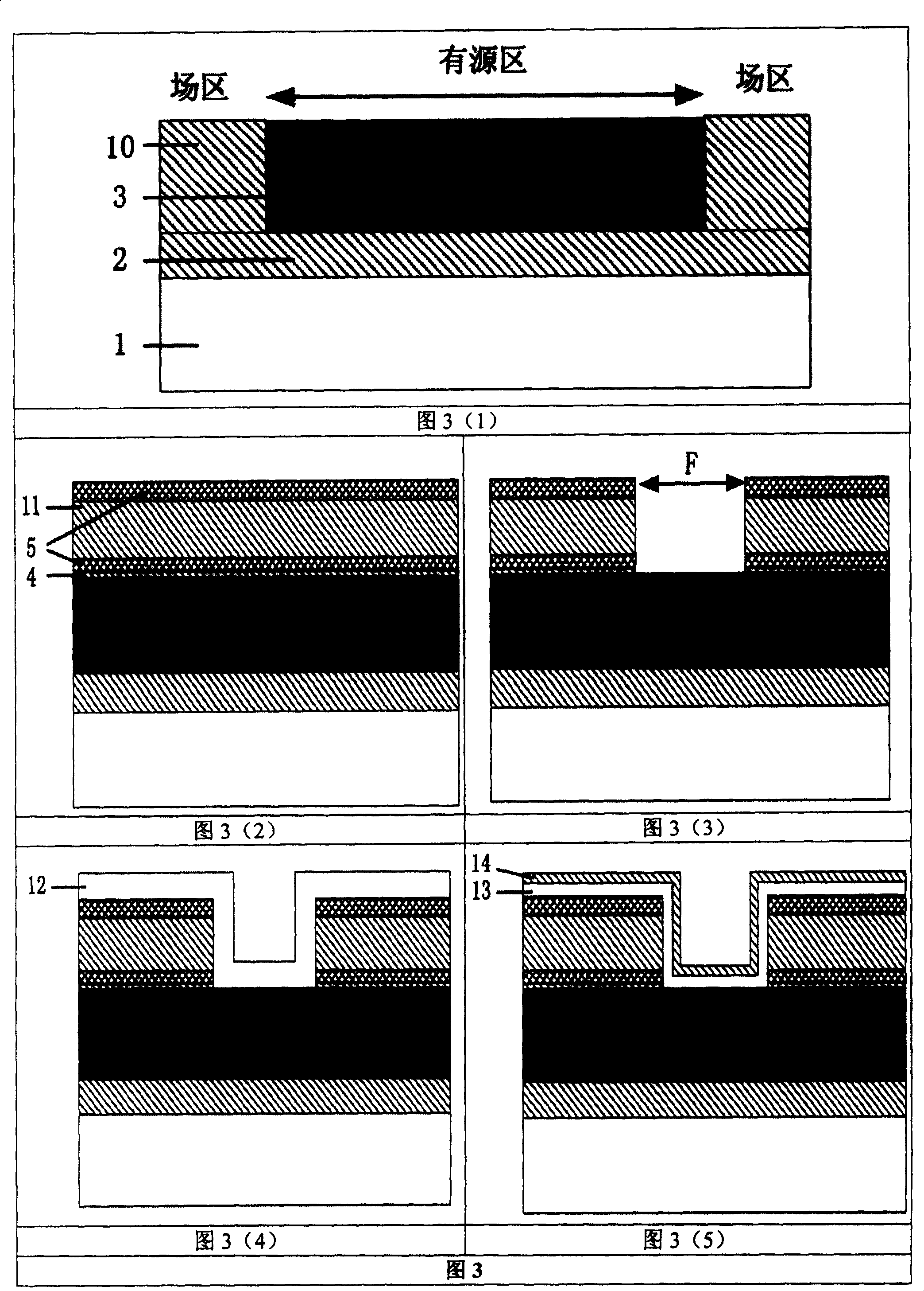
[0025] An implementation method for preparing the above-mentioned vertical channel field effect transistor with a fully depleted double-gate structure will be described in detail bel...


PUM


Abstract

A total exhaust vertical channel double-grating field transistor has two characters: a total exhaust vertical channel double-grating structure, the length and thickness of the channel can be controlled accurately not relaying on the photoetch technology and two double-grating parallel total exhaust channels can be realized on a unit so as to increase the open state drive current. This invention also puts forward a preparation method replacing a grating technology, the technology with Ge as the sacrificial layer, corrupt and epitaxial selection.

Description

technical field [0001] The present invention relates to a kind of field-effect transistor and its manufacturing method, especially a kind of vertical channel field-effect transistor of novel double-gate structure and its manufacturing method, belong to the field-effect transistor (MOSFET—— Metal Oxide Silicon Field Effect Transistor (referred to as MOSFET) structure and its manufacturing technology field. Background technique [0002] With the rapid development of traditional planar CMOS VLSI technology, the feature size of MOSFET devices has entered the era of submicron and deep submicron (<0.1 micron), but the further reduction of device size will be limited by optical lithography technology; The minimum resolution of the currently known most advanced optical lithography technology is 0.157 microns (the smallest optical lithography size, also called feature size, feature size, abbreviated as F). The proposal of the vertical channel field effect transistor opens up a ne...

Claims


Application Information

Patent Timeline
Patent Type & Authority Patents(China)
IPC IPC(8): H01L29/78H01L21/336
Inventor 周发龙黄如蔡一茂张大成张兴王阳元
Owner PEKING UNIV
Why Eureka
Try Eureka