Method of improved high K dielectric - polysilicon interface for CMOS devices

Inactive Publication Date: 2006-06-29
MICRON TECH INC
View PDF27 Cites 2 Cited by
  • Summary
  • Abstract
  • Description
  • Claims
  • Application Information

AI Technical Summary

Benefits of technology

[0011] In addition, the process of the invention results in reduced electrical thickness of the interface layer in a capacitor construction, and thus increased capacitance without adversely affecting the leakage (defectivity) of the stack. The present process achieves more capacitance with the same or re

Problems solved by technology

Despite the advantages of high dielectric constant materials, difficulties have been encountered, however, in incorporating insulating inorganic metal oxide materials into semiconductor fabrications.
The subsequent treatment processes invariably oxidize t

Method used


Image

  • Method of improved high K dielectric - polysilicon interface for CMOS devices
  • Method of improved high K dielectric - polysilicon interface for CMOS devices
  • Method of improved high K dielectric - polysilicon interface for CMOS devices

Examples


Embodiment Construction

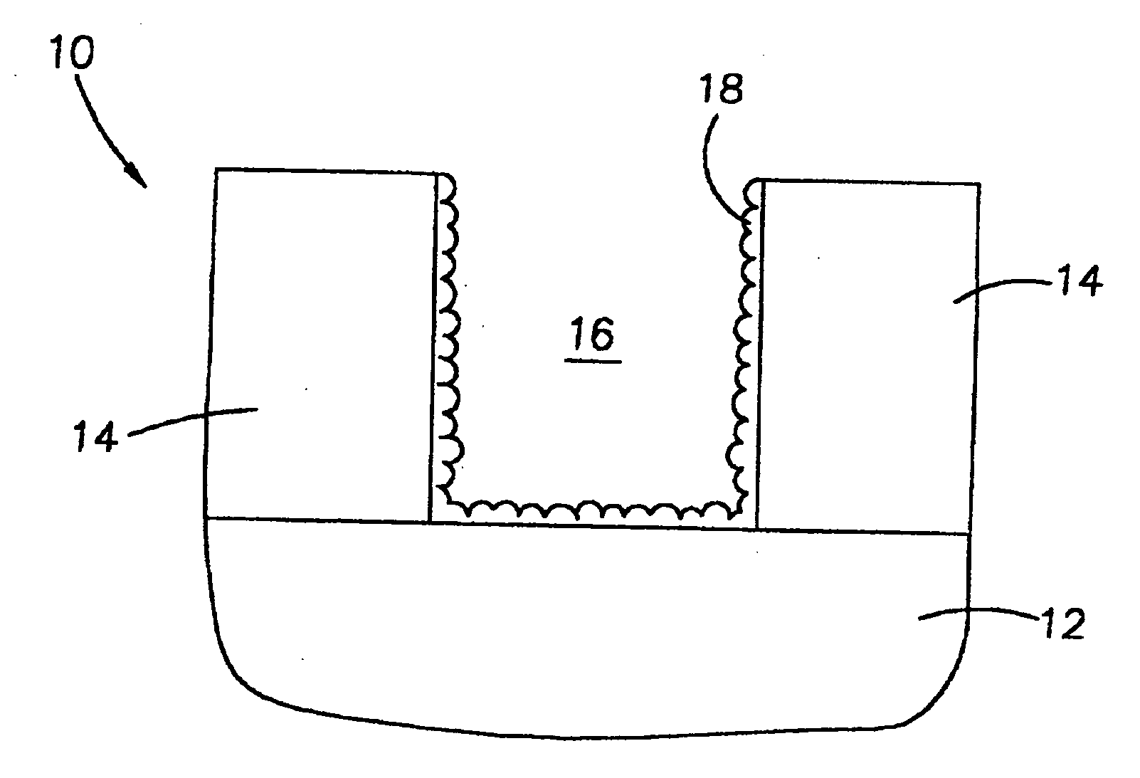
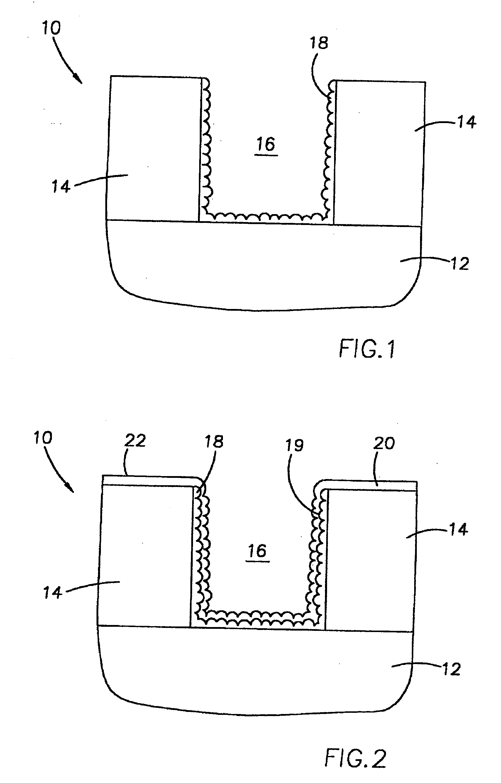
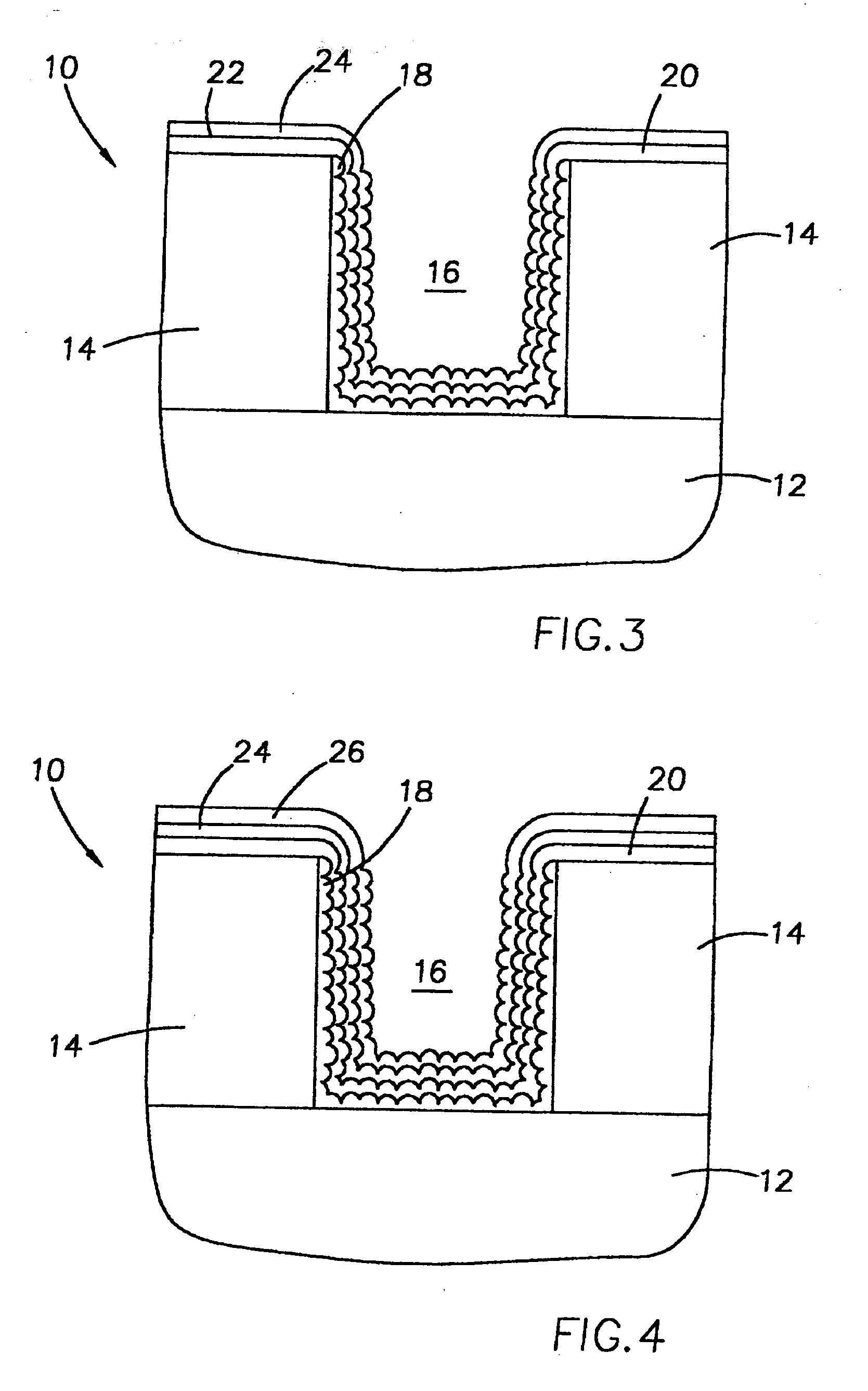
[0022] The invention will be described generally with reference to the drawings for the purpose of illustrating the present preferred embodiments only and not for purposes of limiting the same. The figures illustrate processing steps for use in the fabrication of semiconductor devices in accordance with the present invention. It should be readily apparent that the processing steps are only a portion of the entire fabrication process.

[0023] In the current application, the terms “semiconductive wafer fragment” or “wafer fragment” or “wafer” will be understood to mean any construction comprising semiconductor material, including but not limited to bulk semiconductive materials such as a semiconductor wafer (either alone or in assemblies comprising other materials thereon), and semiconductive material layers (either alone or in assemblies comprising other materials). The term “substrate” refers to any supporting structure including, but not limited to, the semiconductive wafer fragment...


PUM


Abstract

Methods for forming dielectric layers over polysilicon substrates, useful in the construction of capacitors and other semiconductor circuit components are provided. A self-limiting nitric oxide (NO) anneal of a polysilicon layer such as an HSG polysilicon capacitor electrode, at less than 800° C., is utilized to grow a thin oxide (oxynitride) layer of about 40 angstroms or less over the polysilicon layer. The NO anneal provides a nitrogen layer at the polysilicon-oxide interface that limits further oxidation of the polysilicon layer and growth of the oxide layer. The oxide layer is exposed to a nitrogen-containing gas to nitridize the surface of the oxide layer and reduce the effective dielectric constant of the oxide layer. The process is particularly useful in forming high K dielectric insulating layers such as tantalum pentoxide over polysilicon. The nitridized oxynitride layer inhibits oxidation of the underlying polysilicon layer in a post-treatment oxidizing anneal of the high K dielectric, thus maintaining the oxide layer as a thin layer over the polysilicon layer.

Description

CROSS-REFERENCE TO RELATED APPLICATION [0001] This application is a divisional of U.S. patent application Ser. No. 09 / 941,827, filed Aug. 29, 2001.FIELD OF THE INVENTION [0002] The present invention relates generally to semiconductor fabrication and, more particularly, to dielectric layers used in semiconductor fabrication, and to methods of forming capacitors and semiconductor circuit components. BACKGROUND OF THE INVENTION [0003] The continuing trend in integrated circuits toward densification has led to reduced device dimensions and a decrease in size of components that make up the devices. However, in the fabrication of such devices as MOS transistors (metal-oxide semiconductors, or MIS or metal-insulating semiconductors), and with the trend toward higher performance and processing speeds, storage cells must maintain a minimum storage charge to ensure operation of memory cells. Several techniques have been developed to increase the storage capacity of a capacitor within a limite...

Claims


Application Information

Patent Timeline
IPC IPC(8): H01L21/20H01L21/8242H01L21/02H01L21/314H01L21/316H01L27/08
CPCH01L21/3144H01L21/31604H01L27/0805H01L28/56H01L28/84H01L21/0214H01L21/02183H01L21/0217H01L21/02337H01L21/02332
Inventor WEIMER, RONALD A.
Owner MICRON TECH INC
Why Eureka
Try Eureka