

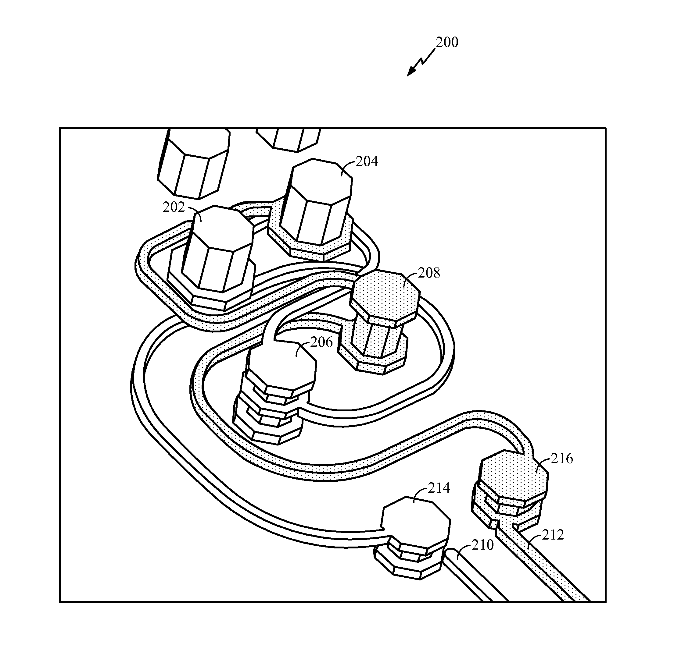
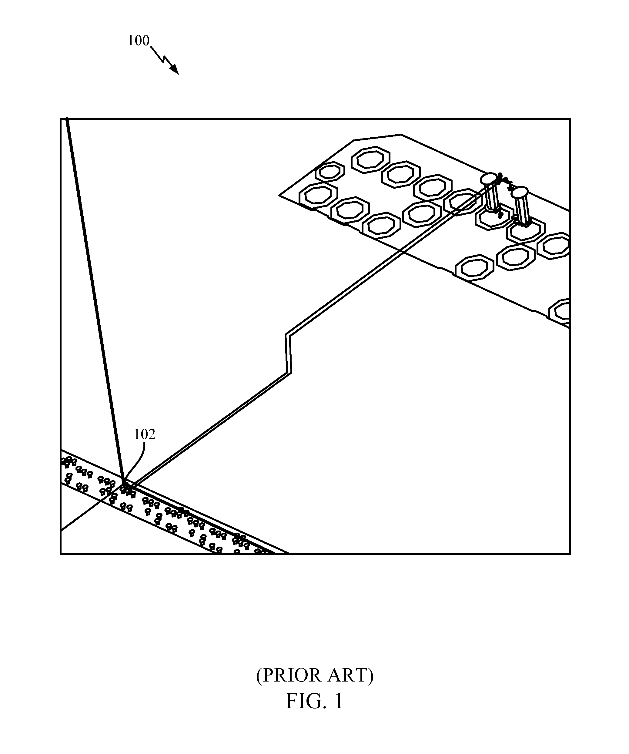
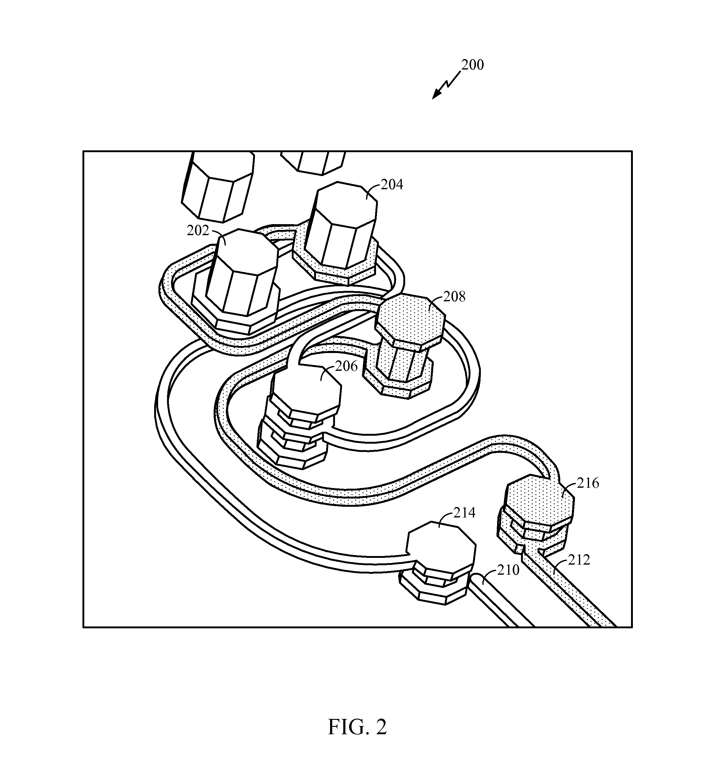
Highly coupled spiral planar inductors structure at bump to compensate on die excess capacitance of differential I/O
a spiral planar inductors and bump technology, applied in the direction of semiconductor devices, semiconductor/solid-state device details, inductances, etc., can solve the problems of large silicon space, system may not deliver the specified amount of performance, and inductors can require a large amount of silicon space, so as to reduce noise
- Summary
- Abstract
- Description
- Claims
- Application Information
AI Technical Summary
Benefits of technology
Problems solved by technology
Method used
Image

Examples
Embodiment Construction
[0019]Various aspects are disclosed in the following description and related drawings. Alternate aspects may be devised without departing from the scope of the disclosure. Additionally, well-known elements of the disclosure will not be described in detail or will be omitted so as not to obscure the relevant details of the disclosure.
[0020]The words “exemplary” and / or “example” are used herein to mean “serving as an example, instance, or illustration.” Any aspect described herein as “exemplary” and / or “example” is not necessarily to be construed as preferred or advantageous over other aspects. Likewise, the term “aspects of the disclosure” does not require that all aspects of the disclosure include the discussed feature, advantage or mode of operation.
[0021]Further, many aspects are described in terms of sequences of actions to be performed by, for example, elements of a computing device. It will be recognized that various actions described herein can be performed by specific circuit...
PUM
 Abstract
Description
Claims
Application Information