Nanopillar arrays for electron emission

a technology of electron emission and nanopillar array, which is applied in the field of nanopillar arrays for electron emission, can solve the problems of incomplete loss of gain functionality, inability to integrate a thin semiconductor membrane as a secondary electron emission element in a detector, and inability to achieve a high gain by integrating multiple stacks, etc., and achieves the effect of low cost and heavy us

Active Publication Date: 2009-12-31
WISCONSIN ALUMNI RES FOUND
View PDF9 Cites 24 Cited by
  • Summary
  • Abstract
  • Description
  • Claims
  • Application Information

AI Technical Summary

Benefits of technology

[0024]Semiconductor membranes and nanopillars useful in specific device embodiments may comprise a variety of doped and undoped semiconductor materials including single crystalline semiconductors, polycrystalline semiconductors, doped diamond, and organic semiconductors. Semiconductor membranes and nanopillars may comprise the same or different semiconductor materials. Semiconductor membranes and nanopillars may comprise a single semiconductor material (doped or undoped), or alternatively may comprise a plurality of semiconductors materials and / or layers. Exemplary semiconductor materials include, but are not limited to, group IV semiconductors such as silicon, germanium and doped diamond, Group IV compound semiconductors, III-V semiconductors, III-V ternary semiconductor alloys, III-V quaternary semiconductor alloys, III-V quaternary semiconductor alloys, II-VI semiconductors, II-VI ternary alloy semiconductors, I-VII semiconductors, IV-VI semiconductors, IV-VI ternary semiconductors, V-VI semiconductors, II-V semiconductors or combinations of these. In an embodiment, the semiconductor membrane, nanopillar or both comprise a carbonaceous materials such as one or graphene or graphite layers (doped or undoped). In an embodiment, the semiconductor membrane, nanopillar or both comprise thin metallic layers and / or semiconductor membranes doped to the metallic limit. In an embodiment, the semiconductor membrane, nanopillar or both comprise SOI (Silicon-on-Insulator), SGOI (Silicon-Germanium-on-lnsulator), or diamond. SOI and similar products (e.g. from SOITEC) are particularly attractive for some embodiments of the present invention as they can be obtained at low cost and are heavily used in the semiconductor industry.

Problems solved by technology

However, most common semiconductors have SEE yield below three, making it impractical to achieve a high gain be integrating multiple stacks.
Providing some semiconductor materials in a semiconductor membrane configuration, for example, results in a complete loss of gain functionality.
Hence, integrating a thin semiconductor membrane as a secondary electron emission element in a detector is currently not feasible for a range of important applications.

Method used


Image

  • Nanopillar arrays for electron emission
  • Nanopillar arrays for electron emission
  • Nanopillar arrays for electron emission

Examples


example 1

Nanopillar Arrays on Semiconductor Membranes Amplify Electron Emission

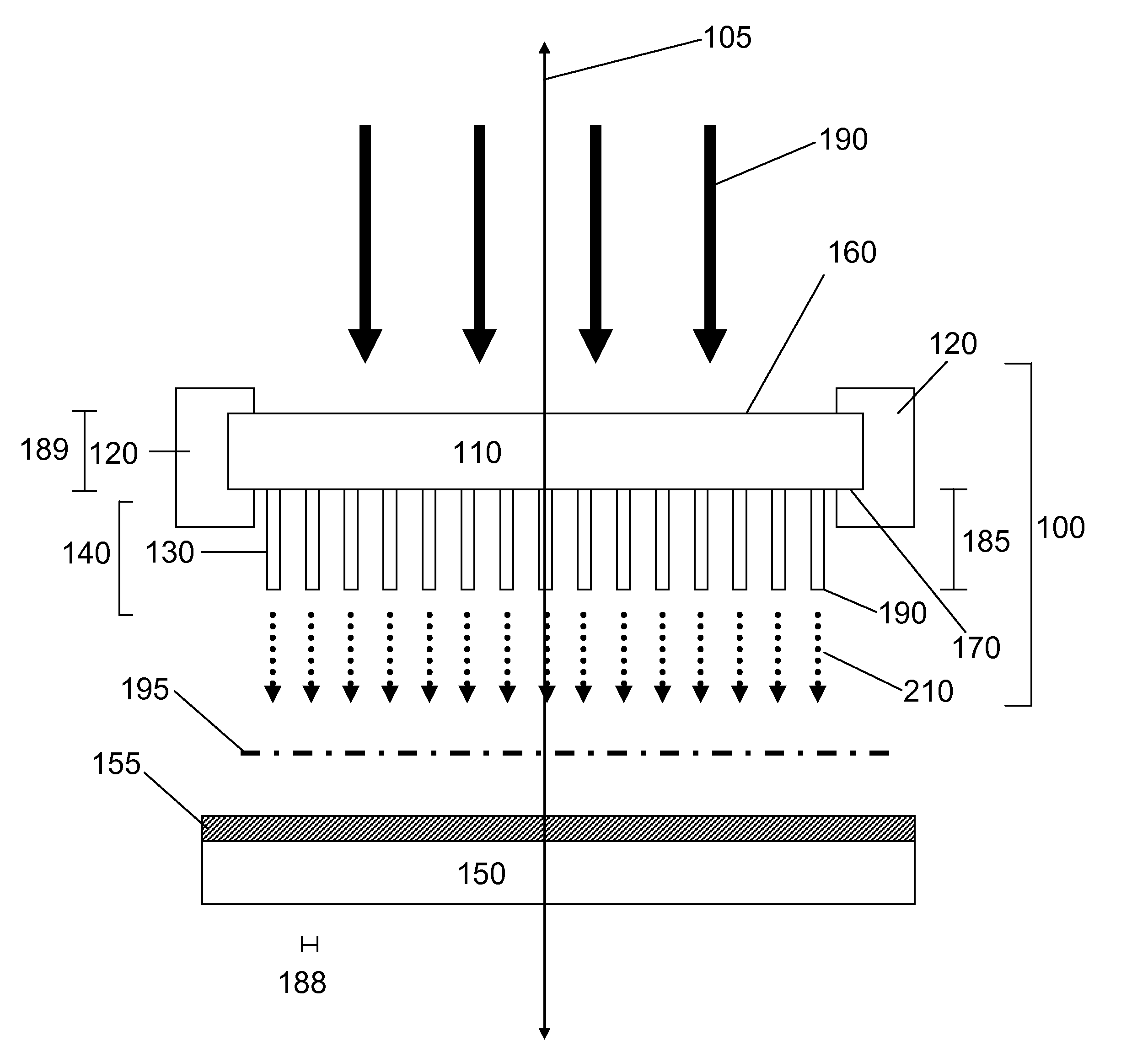
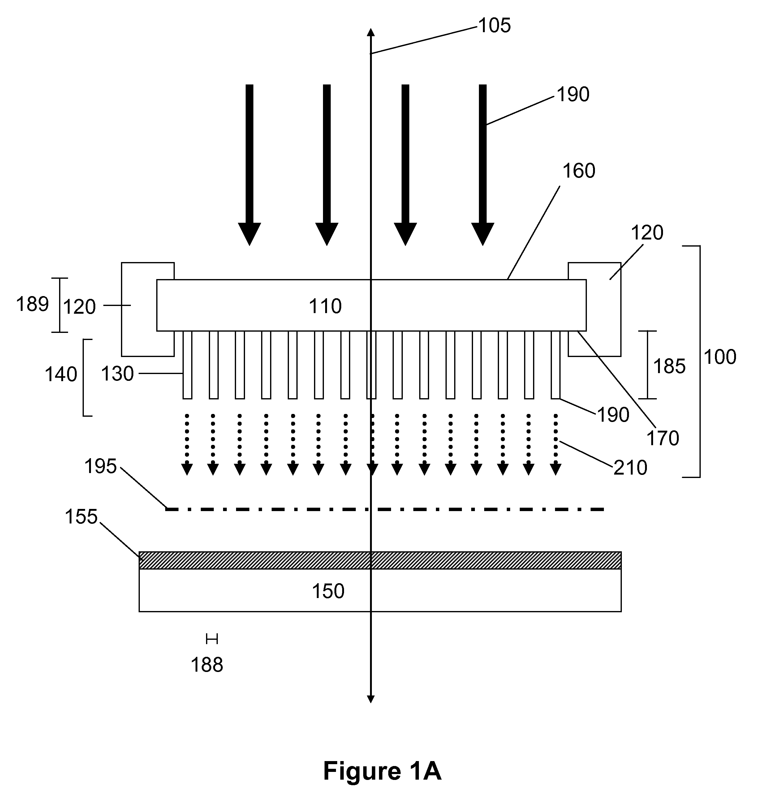
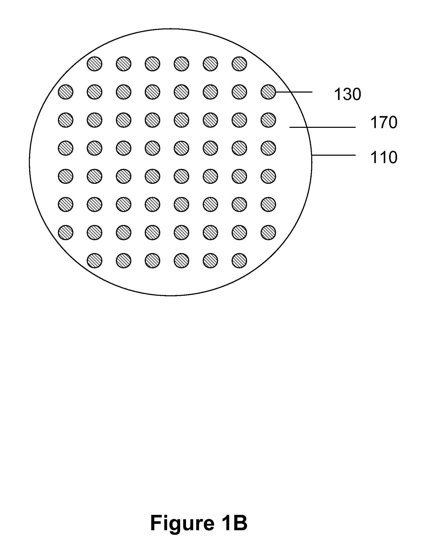
[0071]The present invention provides secondary electron emission devices useful for modulating incident radiation. To evaluate capability of devices of the present invention for generating secondary electron emission, a secondary electron emission device comprising a semiconductor membrane having a nanopillar array was fabricated and exposed to a beam of incident electrons. In this Example experimental results are provided relating to nano-structured single-crystal silicon membranes as the basic element for a new class of active thin-membrane detectors. This integrates the required ‘window’ with the actual detector and thus creates a detector window with gain. As described in this Example, we found that patterning a two-dimensional (2D) membrane with a regular array of one-dimensional (1D) nanopillars strongly enhances SEE generation enabling important applications such as a directed charge amplifier. Further, the...

example 2

Incorporation of a Gaseous Medium within the Nanopillar Arrays

[0084]In some embodiments of the present invention, additional gain in signal is realized by operating the nanopillar array with selected gases, such as a mixture of gases such as Ar, Ne, He, N2, O2, CO2, and CH4 gases, encapsulated between the nanopillar side of the membrane and the collection anode / Faraday cup. In this device configuration, the electrons emitted by the nanopillars are accelerated by the potential difference between the collector and the nanopillar array provided in electrical contact with the internal surface of the semiconductor membrane. If the voltage is adjusted such that the electric field in this region reaches a threshold magnitude, for example 100 kV / cm for a mixture of Ar and CH4 gases, a single electron emerging from a pillar will acquire enough energy to ionize the gas and start an electron cascade, resulting in the generation of 104 to 105 electrons. Embodiments of this aspect of the present...

example 3

Secondary Electron Generation Using an Embedded N P Junction Structure

[0085]The present invention includes electron emission devices having an array of nanopillars comprising embedded N P junction structures. To evaluate the capabilities of nanopillars having embedded N P junction structures, a semiconductor membrane made of silicon and silicon oxide embedded N P junctions was fabricated and exposed to a source of electrons. The results of this Example demonstrate that embedded N P junctions provide useful structures for generating secondary electron emission and field emission.

[0086]Conventional electron multipliers typically have many cascade stages with each stage has a gain of only 1-10 depending on the secondary electron emission (SEE) yield. The semiconductor membrane electron multipliers described in this example are capable of providing a gain larger than 1000 from a single stage comprising a semiconductor membrane as the cathode, an anode and an insulating layer provided be...


PUM

PropertyMeasurementUnit
extraction voltageaaaaaaaaaa
thicknessaaaaaaaaaa
lengthsaaaaaaaaaa

Abstract

The present invention provides systems, devices, device components and structures for modulating the intensity and/or energies of electrons, including a beam of incident electrons. In some embodiments, for example, the present invention provides nano-structured semiconductor membrane structures capable of generating secondary electron emission. Nano-structured semiconductor membranes of this aspect of the present invention include membranes having an array of nanopillar structures capable of providing electron emission for amplification, filtering and/or detection of incident radiation, for example secondary electron emission and/or field emission. Nano-structured semiconductor membranes of the present invention are useful as converters wherein interaction of incident primary electrons and nanopillars of the nanopillar array generates secondary emission. Nano-structured semiconductor membranes of this aspect of the present invention are also useful as directed charge amplifiers wherein secondary emission from a nanopillar array provides gain functionality for increasing the intensity of radiation comprising incident electrons.

Description

CROSS-REFERENCE TO RELATED APPLICATIONS[0001]This application claims the benefit of U.S. Provisional Patent Application 60 / 941,675 filed Jun. 3, 2007, which is hereby incorporated by reference in its entirety to the extent not inconsistent with the disclosure herein.STATEMENT REGARDING FEDERALLY SPONSORED RESEARCH OR DEVELOPMENT[0002]This invention was made with government support awarded by the following agencies: Air Force RSO under contract number F49629-03-1-0420. The United States government has certain rights in the invention.BACKGROUND OF INVENTION[0003]An electron multiplier is a common device component which uses secondary electron emission (SEE) to provide a gain in the intensity of incident radiation. In some device embodiments, for example, incident primary electrons pass a ‘window’ component of the device and scatter with a detector material capable of inducing a cascade of secondary electrons. By proper selection of the composition and physical state of the detector g...

Claims


Application Information

Patent Timeline
Patent Type & Authority Applications(United States)
IPC IPC(8): H01L29/66B01J19/12G01N23/00
CPCH01J1/32H01J43/246H01J29/023Y10S977/762
Inventor BLICK, ROBERT H.WESTPHALL, MICHAEL S.QIN, HUASMITH, LLOYD M.
Owner WISCONSIN ALUMNI RES FOUND
Why Eureka
Try Eureka