Application of semiconductor quantum dot phosphors in nanopillar light emitting diodes

a technology of light-emitting diodes and quantum dots, applied in the field of light-emitting diodes, can solve the problems of difficult mixing and depositing uniform multi-phosphor films, difficult control of granule size, and number of performance limits of white leds, etc., and achieves efficient non-radiative transfer and improved efficiency

Inactive Publication Date: 2013-08-08
PENN STATE RES FOUND
View PDF6 Cites 24 Cited by
  • Summary
  • Abstract
  • Description
  • Claims
  • Application Information

AI Technical Summary

Problems solved by technology

The energy efficiency, longevity, and material usage in manufacture are all attributes that favor white LED technology, yet technical problems persist.
There are, nevertheless, a number of limits on the performance of those white LEDs due to the phosphor conversion scheme employed.
Since the existing red, yellow, and green phosphors have different chemical compositions, it is difficult to control the granule size and to mix and deposit uniform multi-phosphor films.
Also, the different aging behavior of the multiple phosphor species often makes the device performance unstable in terms of the overall wavelength output.
A more fundamental limit on the efficiency of the phosphor conversion white LEDs, however, lies in the multi-step “down conversion” scheme: high energy, blue photons produced by InGaN QW LEDs have to be absorbed by the phosphors first, and then, via impurity-level assisted transitions, are converted to low energy, long wavelength photons with a one-to-one correspondence.
This process loses a significant portion of the photon energy to lattice vibrations (heat) in the phosphor media as a non-radiative conversion and is also limited by electron system crossings between singlet and triplet quantum states.
As promising as the indirect injection of electron hole pairs into QD approach appears to be, it has to-date met with limit success.
Since the QDs were physically separated from the emissive QWs in the LED chip, no QW-QD coupling was possible.
The viability of this work was limited in producing an actual LED device owing to the difficulty in resolving the inherent conflict between the need for close proximity of the QW and QDs and also the need for a sufficiently thick electrical contact layer with a low resistance for LED operation.
In addition, the energy fraction (13%) channeled between the QW and QDs is still too low for viable device formation to leverage the benefits of white LEDS relative to conventional lighting devices.
These experimental devices with weak QD phosphor emission compared to the bright blue radiation from the InGaN QW remain impractical for usage.

Method used


Image

  • Application of semiconductor quantum dot phosphors in nanopillar light emitting diodes
  • Application of semiconductor quantum dot phosphors in nanopillar light emitting diodes
  • Application of semiconductor quantum dot phosphors in nanopillar light emitting diodes

Examples


example 1

Fabrication of InGaN / GaN Based Nanopillar LEDs

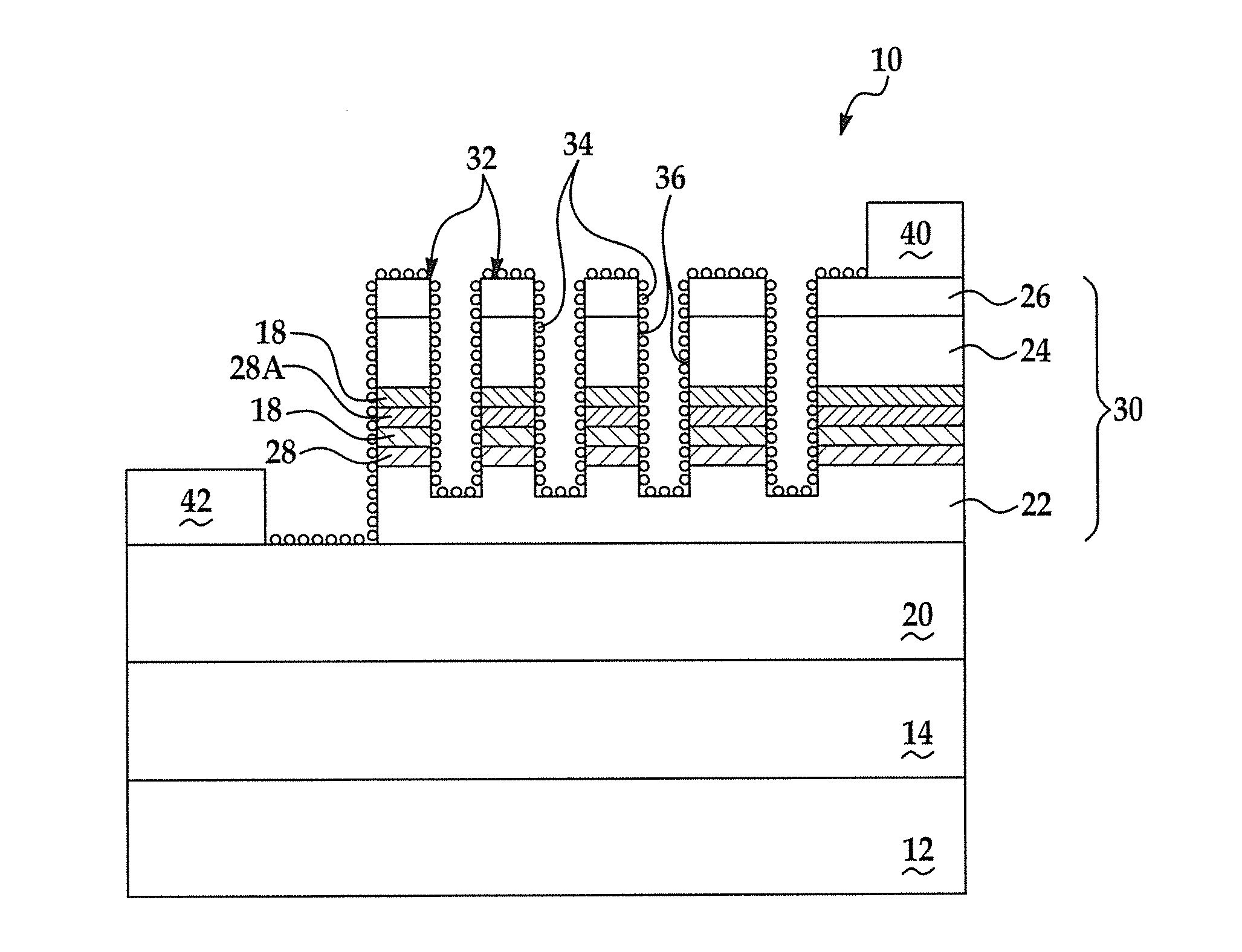
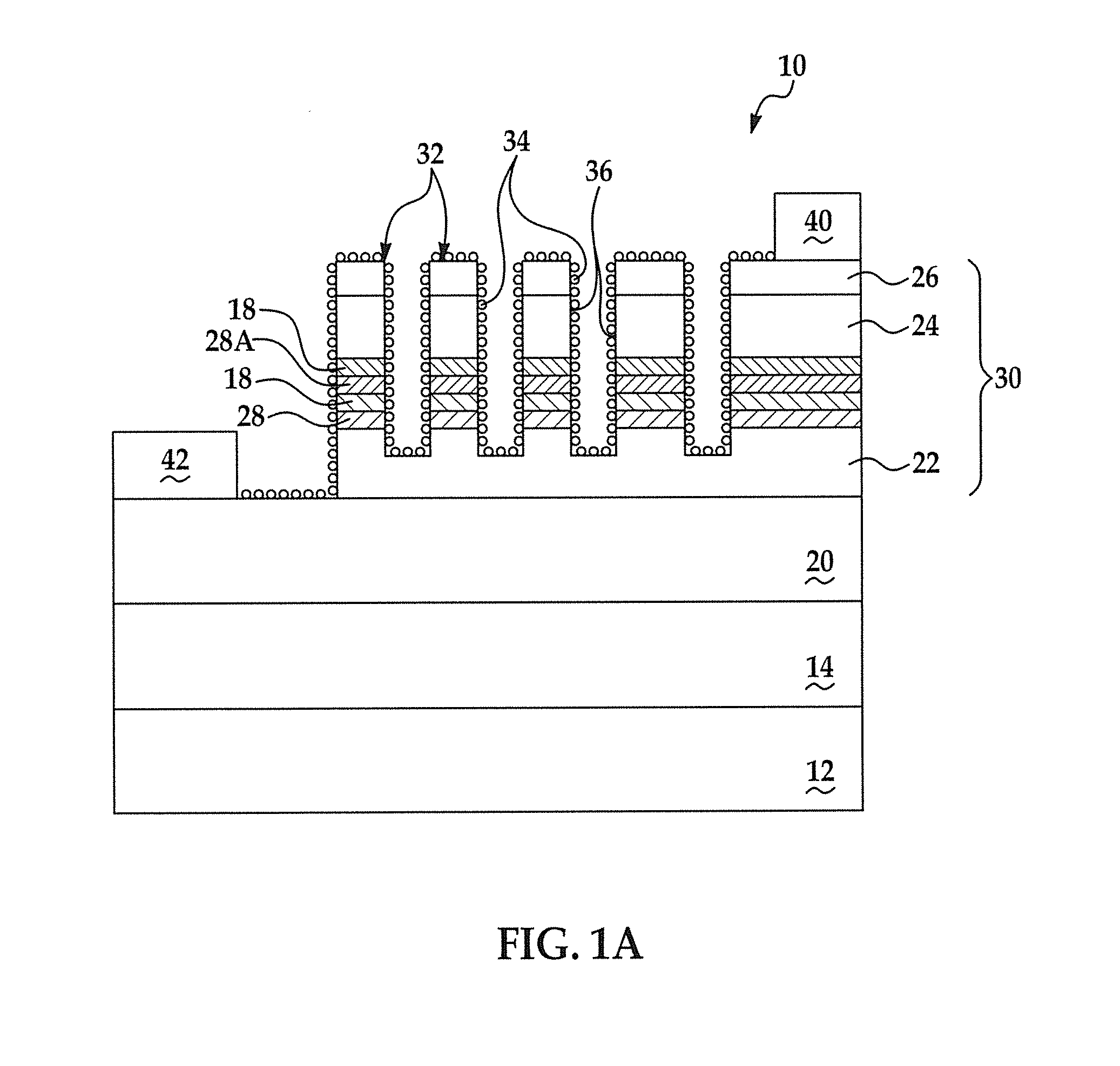
[0028]High density InGaN / GaN based nanopillar LEDs were fabricated by using self-assembled tin oxide (TO) nanodots and dry etching the InGaN / GaN using the TO nanodots as a mask. The self-assembled TO nanodots were produced as follows. A SiO2 layer was deposited on the top surface of the LED wafer using a plasma-enhanced chemical vapor deposition (PECVD) system, and then an indium tin oxide (ITO) layer was deposited onto the SiO2 layer using an electron beam evaporator. The sample with the LED wafer / SiO2 / ITO layers was dipped into a solution containing HCl to etch away indium oxide clusters, which gave rise to self-assembled tin oxide clusters on the SiO2 layer. The SiO2 layer was then etched using the tin oxide clusters as an etching mask. After the patterning of the SiO2 layer, the etching mask of the oxide clusters was removed using a chemical solution. Then, the LED wafer was dry-etched using the SiO2 clusters as an etch mask. Finally...

example 2

Fabrication of QD Coated Nanopillar LEDs

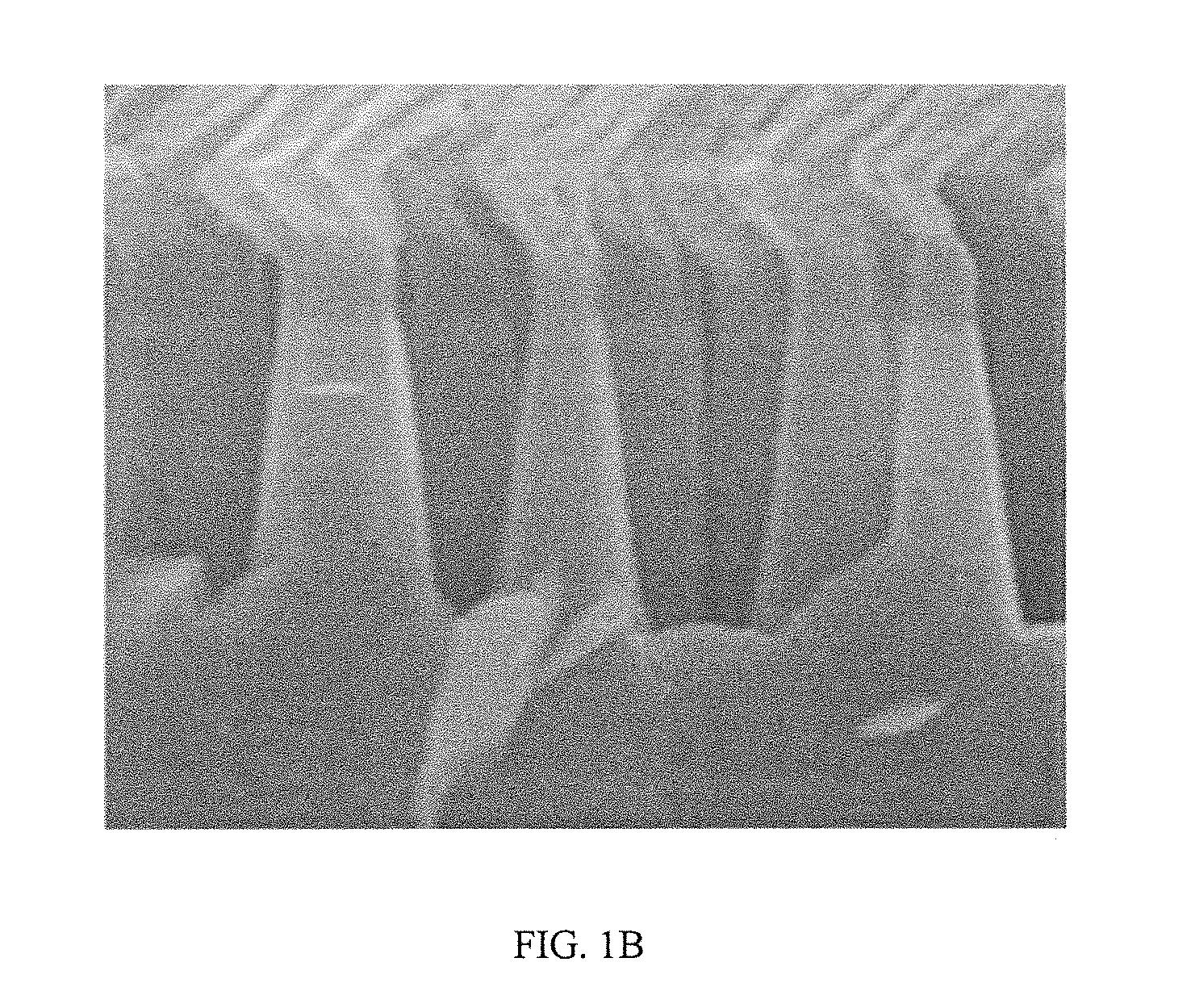
[0029]The InGaN / GaN MQW LED nanopillars were fabricated by the inductively coupled plasma (ICP) etching using self-assembled TO nanodots as the etching mask with the PL peak centered at 460 nm. By controlling the size of the TO nanodots and the ICP etching time, nanorods with a height of 500 nm and diameters ranging between 100 nm and 500 nm were fabricated successfully. A layer of CdSe / CdS core / shell QDs with the PL peak centered at 620 nm were coated over the nanopillar LED sample and subsequently annealed at 100° C. to remove the solvent. (The coating methods include soaking the nanopillar LED into the QD solution, spin-casting, drop-casting or mist deposition.) FIG. 1B is a cross sectional scanning electron microscopy image of the device so formed. FIG. 2A shows a field emission scanning electron microscopy (FESEM) image of a QD-coated nanopillar LED sample. FIG. 2B shows the z-scan 3D confocal fluorescent microscope image of the QD phosph...

example 3

Characterization of QD Coated Nanopillar LEDs

[0030]To study the direct MWQ to QD nonradiative energy transfer rate, time-resolved photoluminescence (TRPL) studies were performed for the InGaN nanorod LED structure of Example 1 with and without colloidal QD coating per Example 2. Two identical nanopillar LED samples with ˜200 nm nanopillar diameter were used for the measurement. Both samples coated with and without QD phosphors were excited by the second harmonic (λ=400 nm) of a femtosecond light source (Libra, Coherent Inc., 70 fs pulse duration, 1 kHz repetition rate, 1 mJ pulse energy at λ=800 nm). The photoluminescence (PL) signal from the MQW region of the nanorods was collected by a photomultiplier by passing through a band pass filter (460 / 10 nm). The time resolution of the whole system was about 10 ps. All measurements were performed at room temperature.

[0031]FIG. 3 shows the PL spectra of the two investigated nanorod LED samples coated with and without QD phosphors. The rela...


PUM

PropertyMeasurementUnit
heightaaaaaaaaaa
heightaaaaaaaaaa
quantum efficiencyaaaaaaaaaa

Abstract

A quantum well-based p-i-n light emitting diode is provided that includes nanopillars with an average linear dimension of between 50 nanometers and 1 micron. The nanopillars include a laminar layer of quantum wells capable of non-radiative energy transfer to quantum dot nanocrystals. Quantum dot-Quantum well coupling through the side walls of the nanopillar-configured LED structure achieves a close proximity between quantum wells and quantum dots while retaining the overlying contact electrode structures. A white LED with attractive properties relative to conventional incandescent and fluorescence lighting devices is produced.

Description

REFERENCE TO RELATED APPLICATIONS[0001]This application claim priority from United States Provisional Application Ser. No. 61 / 587,884 filed Jan. 18, 2012; the contents of which are hereby incorporated by reference.STATEMENT OF GOVERNMENT SUPPORT[0002]This invention was made with government support under Grant No. ECCS0824186, awarded by the National Science Foundation. The Government has certain rights in the invention.FIELD OF THE INVENTION[0003]The present invention relates in general to a light emitting diode (LED) and in particular to a white light LED based on semiconductor quantum dots (QDs) used as phosphors in nanopillar LEDs.BACKGROUND OF THE INVENTION[0004]White light emitting diode (LED) based solid-state lighting is commanding much attention worldwide for its promise of energy savings compared to incandescent and even compact fluorescent lighting. The energy efficiency, longevity, and material usage in manufacture are all attributes that favor white LED technology, yet t...

Claims


Application Information

Patent Timeline
Patent Type & Authority Applications(United States)
IPC IPC(8): H01L33/04
CPCH01L33/04B82Y99/00B82Y10/00H01L33/502H01L33/06H01L33/20B82Y20/00
Inventor ZHANG, FANXU, JIANMOHNEY, SUZANNE
Owner PENN STATE RES FOUND
Why Eureka
Try Eureka