

Multiple signal format output driver with configurable internal load
a multi-signal format and output driver technology, applied in logic circuits, logic circuit coupling/interface arrangements, pulse techniques, etc., can solve the problems of significant degrading system performance, conversion buffers introduce additional board space and clock jitter costs, and introduce additional mask costs
- Summary
- Abstract
- Description
- Claims
- Application Information
AI Technical Summary
Benefits of technology
Problems solved by technology
Method used
Image

Examples
Embodiment Construction
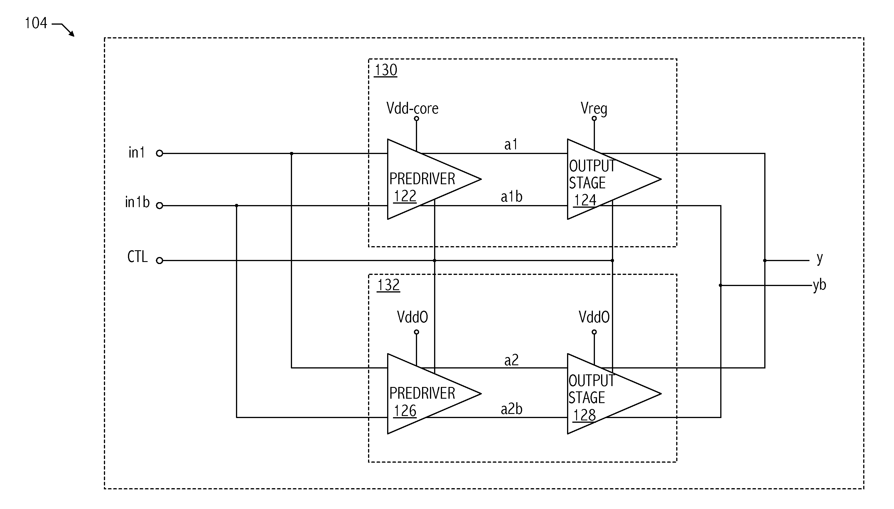
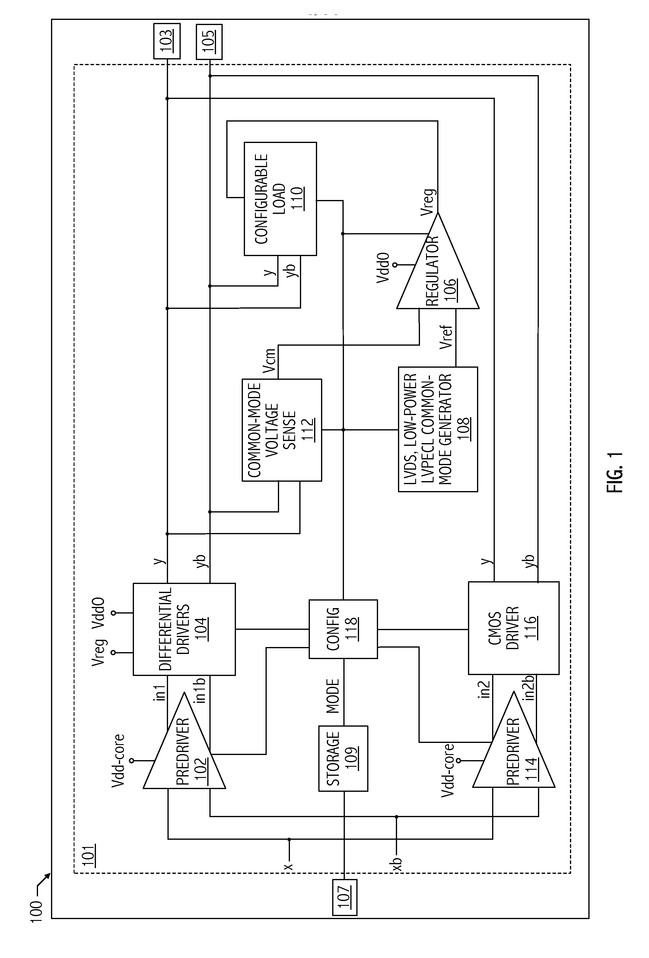
[0008]In at least one embodiment of the invention, an integrated circuit includes a first output node and a second output node. The integrated circuit includes a multiple signal format output driver, which includes a differential circuit configured to provide a differential signal to the first output node and the second output node. The multiple signal format output driver includes a load circuit including a first resistor and a second resistor. The load circuit is configurable in response to one or more first values of a control signal to couple the first resistor between the first output node and a regulated voltage node and to couple the second resistor between the second output node and the regulated voltage node. The load circuit is configurable in response to one or more second values of the control signal to couple the first and second output nodes to each other using the first and second resistors. In at least one embodiment of the integrated circuit, the multiple signal for...
PUM
 Abstract
Description
Claims
Application Information