Packaging method

a technology of semiconductors and packaging, applied in the field of semiconductor technology, can solve the problems of significant reduction of chip size and chip cost, and achieve the effects of reducing interference factors, facilitating the localization of mounting chips, and high integrity

Active Publication Date: 2013-11-14
NANTONG FUJITSU MICROELECTRONICS
View PDF6 Cites 8 Cited by
  • Summary
  • Abstract
  • Description
  • Claims
  • Application Information

AI Technical Summary

Benefits of technology

[0011]In the packaging method in one embodiment of the present disclosure, since the chip and the passive device are integrated and packaged together, the packaging structure is a packaging product including whole-system functions but not single-chip functions. Compared with conventional system-level packaging structures, the packaging structure in the present disclosure has high integrity, decreases interference factors in a system, such as resistors or inductors, and goes with the trend that semiconductor packaging is becoming light, thin and short.
[0012]In the packaging method in one embodiment of the present disclosure, the shape and position of the adhesive layer formed on the carrier board may correspond to the shapes of the functional surfaces of the devices to be packaged and the positions on the carrier board where the devices to be packaged are to be attached, respectively, which facilitates the localization of mounting chips and avoids difficulty in peeling or widespread cleaning in subsequent processes.
[0013]In the packaging method in one embodiment of the present disclosure, the whole packaging of the sealing material layer is divided into a plurality of small packaged blocks to reduce the inner stress of the sealing material layer, which avoids warp and distortion of the sealing material layer in subsequent processes during wafer packaging and improves the quality of wafer packaging products.

Problems solved by technology

Packaging with the WLCSP technology realizes high miniaturization, and the chip cost decreases significantly with the decrease of the chip size and the increase of the wafer size.

Method used


Image

  • Packaging method
  • Packaging method
  • Packaging method

Examples


first embodiment

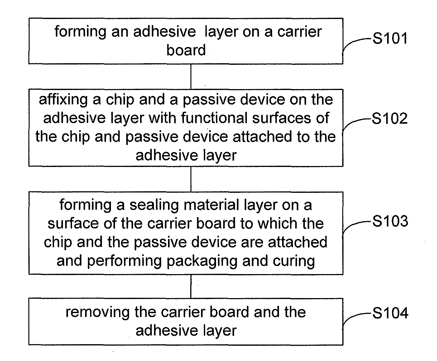
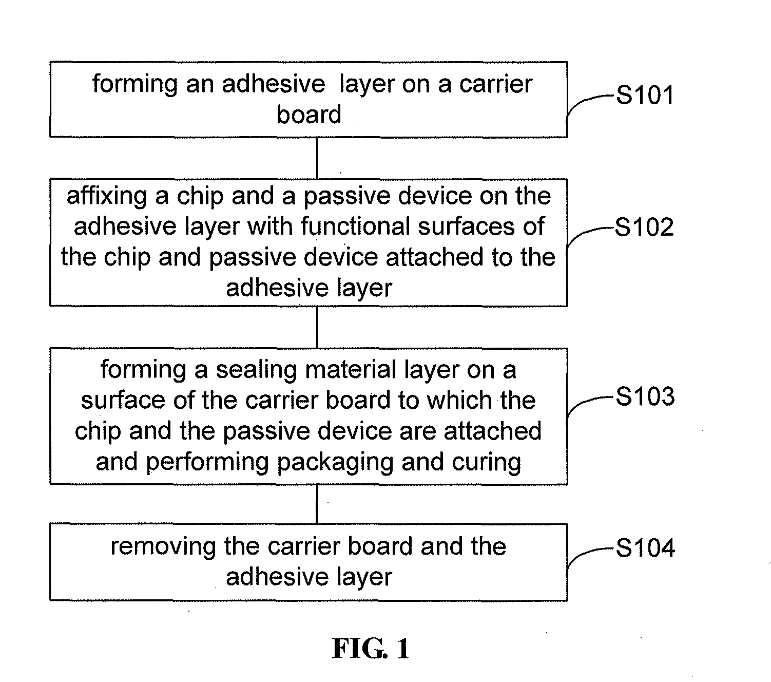
[0028]As shown in FIG. 1, in the present disclosure, a packaging method may include following steps:

[0029]S101, forming an adhesive layer on a carrier board;

[0030]S102, affixing a chip and a passive device on the adhesive layer with functional surfaces of the chip and passive device attached to the adhesive layer;

[0031]S103, forming a sealing material layer on a surface of the carrier board to which the chip and the passive device are attached and performing packaging and curing; and

[0032]S104, removing the carrier board and the adhesive layer.

second embodiment

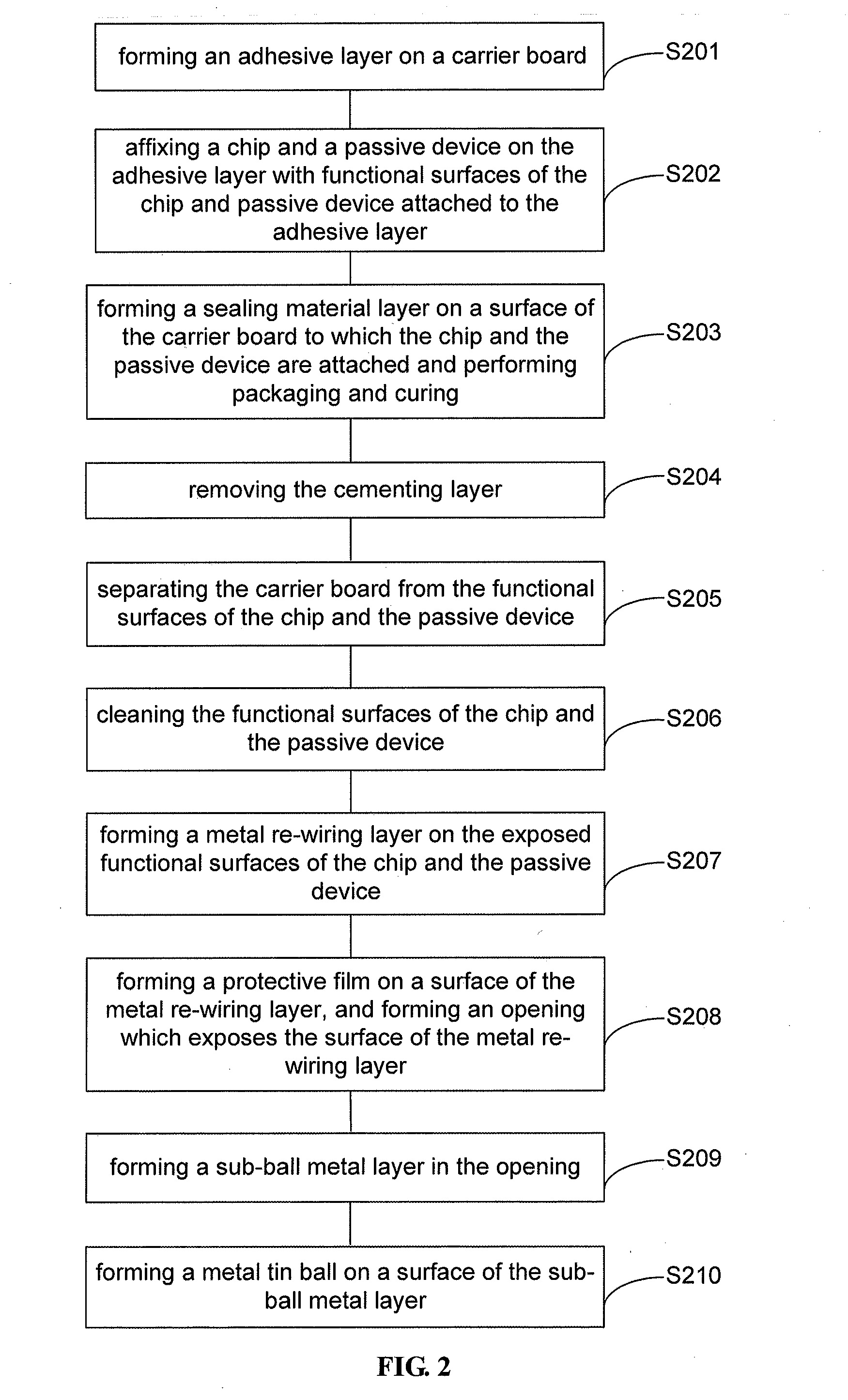
[0033]As shown in FIG. 2, in the present disclosure, a packaging method may include following steps:

[0034]S201, forming an adhesive layer on a carrier board;

[0035]S202, affixing a chip and a passive device on the adhesive layer with functional surfaces of the chip and passive device attached to the adhesive layer;

[0036]S203, forming a sealing material layer on a surface of the carrier board to which the chip and the passive device are attached and performing packaging and curing;

[0037]S204, removing the adhesive layer;

[0038]S205, separating the carrier board from the functional surfaces of the chip and the passive device;

[0039]S206, cleaning the functional surfaces of the chip and the passive device;

[0040]S207, forming a metal re-wiring layer on the exposed functional surfaces of the chip and the passive device;

[0041]S208, forming a protective film on a surface of the metal re-wiring layer, and forming an opening which exposes the surface of the metal re-wiring layer;

[0042]S209, for...

third embodiment

[0063]As shown in FIG. 11, in the present disclosure, a packaging method may include following steps: S301, forming an adhesive layer on a carrier board, where a shape and position of the adhesive layer may correspond to shapes of functional surfaces of devices to be packaged and positions on the carrier board where the devices to be packaged are to be attached, respectively;

[0064]S302, affixing a chip and a passive device on the adhesive layer with functional surfaces of the chip and passive device attached to the adhesive layer;

[0065]S303, forming a sealing material layer on a surface of the carrier board to which the chip and the passive device are attached and performing packaging and curing; and

[0066]S304, removing the carrier board and the adhesive layer.


PUM


Abstract

The present invention relates to a packaging method including the steps: a cementing layer is formed on a carrier board; the functional sides of chips and passive devices are attached to the cementing layer; a sealing material layer is formed on the side of the carrier board to which the chips and the passive devices are attached, and packaging and curing are performed; and the carrier board and the cementing layer are removed. Compared to the prior art, the system-level fan-out wafer packaging method claimed by the present invention first integrates chips and passive devices and then packages the chips and the passive devices together, thereby forming a final packaged product having not single-chip functionality but integrated-system functionality. Compared to current system-level packaging, highly integrated wafer-level packaging reduces such interfering factors as system-internal electric resistance and inductance, and accommodates the growing demand for lighter, thinner, shorter, and smaller semiconductor packaging.

Description

CROSS-REFERENCE TO RELATED APPLICATIONS[0001]The present application claims priority to Chinese patent application No. 201110032270.7, filed on Jan. 30, 2011, and entitled “SYSTEM-LEVEL FAN-OUT WAFER PACKAGING METHOD”, Chinese patent application No. 201110032676.5, filed on Jan. 30, 2011, and entitled “HIGH-DENSITY SYSTEM-LEVEL CHIP PACKAGING METHOD”, and Chinese patent application No. 201110032591.7, filed on Jan. 30, 2011, and entitled “HIGH-INTEGRITY WAFER FAN-OUT PACKAGING METHOD”, and the entire disclosures of which are incorporated herein by reference.FIELD OF THE DISCLOSURE[0002]The present disclosure generally relates to semiconductor technology, and more particularly, to a packaging method.BACKGROUND OF THE DISCLOSURE[0003]Wafer Level Packaging (WLP) is a technology in which a whole wafer is packaged and tested, and then diced into individual chips. The size of a packaged chip is almost the same as that of a bare chip. Wafer Level Chip Size Packaging (WLCSP) technology is t...

Claims


Application Information

Patent Timeline
Patent Type & Authority Applications(United States)
IPC IPC(8): H01L21/52H01L21/56
CPCH01L21/52H01L21/568H01L21/561H01L23/3128H01L23/49816H01L23/5389H01L24/19H01L24/96H01L2924/1815H01L24/20H01L2224/24195H01L2924/19105H01L2224/04105H01L2224/12105H01L2924/181H01L2924/12042H01L2924/3511H01L2924/00012H01L2924/00
Inventor TAO, YUJUANSHI, LEIGAO, GUOHUASHI, JIANGENZHU, HAIQING
Owner NANTONG FUJITSU MICROELECTRONICS
Why Eureka
Try Eureka