Wafer level optical sensor package and low profile camera module, and method of manufacture

a technology of optical sensor and low-profile camera, applied in the field of wafer-level packages, can solve the problems of incompatibility with the correct operation of optical sensor, less desirable use for small electronic devices, and potential light leakag

Active Publication Date: 2013-12-05
STMICROELECTRONICS PTE LTD
View PDF4 Cites 57 Cited by
  • Summary
  • Abstract
  • Description
  • Claims
  • Application Information

AI Technical Summary

Benefits of technology

[0048]Another advantage is that because the sensor die and other associated electronic elements are embedded together in the molding compound layer and electrically coupled by the redistribution layer, the elements can be positioned much more compactly, so that even though the sensor package includes a portion of the molding compound layer, it can occupy less circuit board space than a camera module and associated elements of the prior art. Additionally, the molding compound layer, which is opaque, eliminates the possible sources of light leaks that are often present in the prior art.

Problems solved by technology

A challenge that designers face with respect to coupling the optical sensor to a camera circuit is that the device must be positioned on a substrate with the optical sensor facing outward, and without any obstructions that would interfere with the reception of an optical image.
It is therefore necessary to couple a circuit to contact pads that are not overlying the optical sensor using techniques that are often not compatible with the correct operation of the optical sensor.
The example of FIG. 1 is problematic because the housing must be high enough and wide enough to accommodate the wirebonds 28, which makes it less desirable for use in small electronic devices because it limits the minimum thickness of such devices.
Nevertheless, there are some problems associated with the configuration shown in FIG. 2, including the potential for light leaks.

Method used


Image

  • Wafer level optical sensor package and low profile camera module, and method of manufacture
  • Wafer level optical sensor package and low profile camera module, and method of manufacture
  • Wafer level optical sensor package and low profile camera module, and method of manufacture

Examples


Embodiment Construction

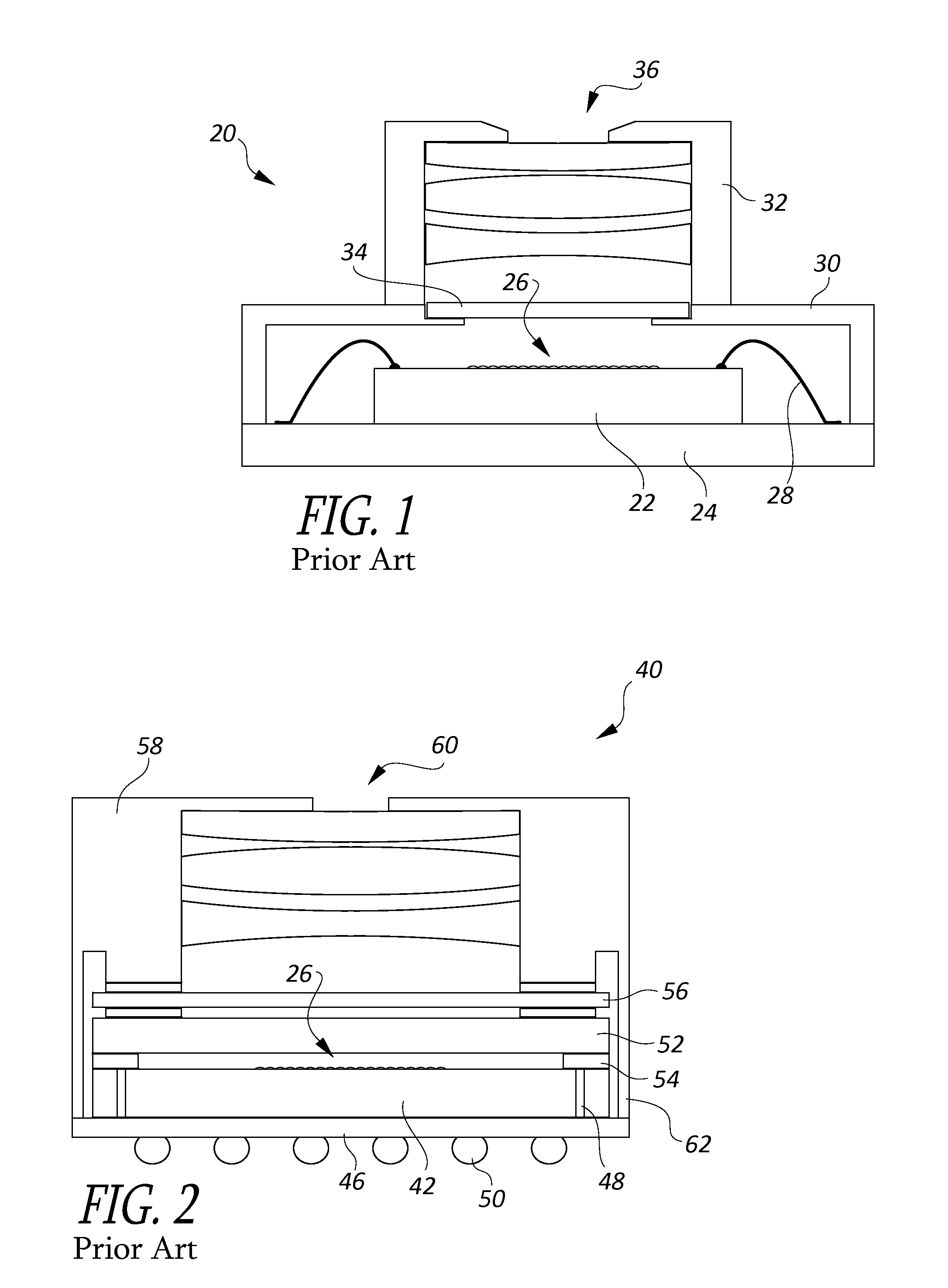
[0024]While the prior art example of FIG. 2 has a reduced height, relative to the example of FIG. 1, the inventors have recognized that there are a number of problems that can be associated with the second example. First, the associated semiconductor wafer and glass cover must be thinned to their final thicknesses before the wafer is singulated into individual dice. However, If they are too thin, they become extremely fragile, and can break during singulation. Also, handling of the glass and die assembly by assembly workers or automatic machinery used to assemble the camera module can easily damage them. Additionally, planarity becomes a problem, because the thinned die can be flexed slightly during assembly, resulting in an optical sensor that does not function properly or produces distorted images. Another problem is light leaks. If the lens assembly is not perfectly light tight, or if any light scatter occurs inside the lens assembly, the light can be transmitted from the edge of...


PUM


Abstract

A wafer-level camera sensor package includes a semiconductor substrate with an optical sensor on a front surface. Through-silicon-vias (TSV) extend through the substrate and provide I / O contact with the sensor from the back side of the substrate. A glass cover is positioned over the front surface, and the cover and substrate are embedded in a molding compound layer (MCL), the front surface of the MCL lying coplanar with the front of the cover, and the back surface lying coplanar with the back of the substrate. Surface-mount devices, electromagnetic shielding, and through-wafer-connectors can be embedded in the MCL. A redistribution layer on the back surface of the MCL includes bottom contact pads for mounting the package, and conductive traces interconnecting the contact pads, TSVs, surface-mount devices, shielding, and through-wafer-connectors. Anisotropic conductive adhesive is positioned on the front of the MCL for physically and electrically attaching a lens array.

Description

BACKGROUND[0001]1. Technical Field[0002]Embodiments of the present invention are directed to a wafer-level package for an optical sensor device, and in particular to a package in which a sensor assembly is embedded in a molding compound layer, and also to a camera module that includes such a package.[0003]2. Description of the Related Art[0004]A challenge that designers face with respect to coupling the optical sensor to a camera circuit is that the device must be positioned on a substrate with the optical sensor facing outward, and without any obstructions that would interfere with the reception of an optical image. It is therefore necessary to couple a circuit to contact pads that are not overlying the optical sensor using techniques that are often not compatible with the correct operation of the optical sensor. Additionally, as camera modules are more commonly used in small electronic devices such as cell phones and tablet computers, there is a strong market pressure to reduce th...

Claims


Application Information

Patent Timeline
Patent Type & Authority Applications(United States)
IPC IPC(8): H01L31/0232H01L31/18
CPCH01L27/14618H01L2924/0002H01L27/14625H01L2924/00
Inventor LUAN, JING-EN
Owner STMICROELECTRONICS PTE LTD
Why Eureka
Try Eureka