

Optical panel and processing method thereof
- Summary
- Abstract
- Description
- Claims
- Application Information
AI Technical Summary
Benefits of technology
Problems solved by technology
Method used
Image

Examples
Embodiment Construction
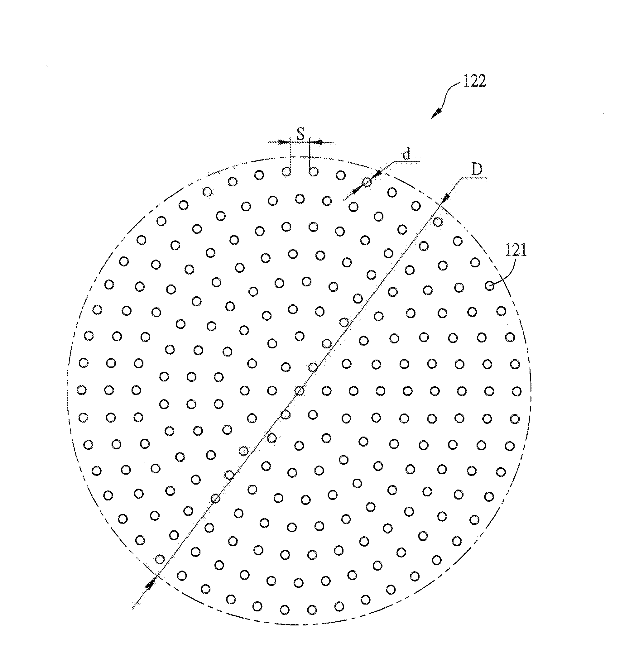
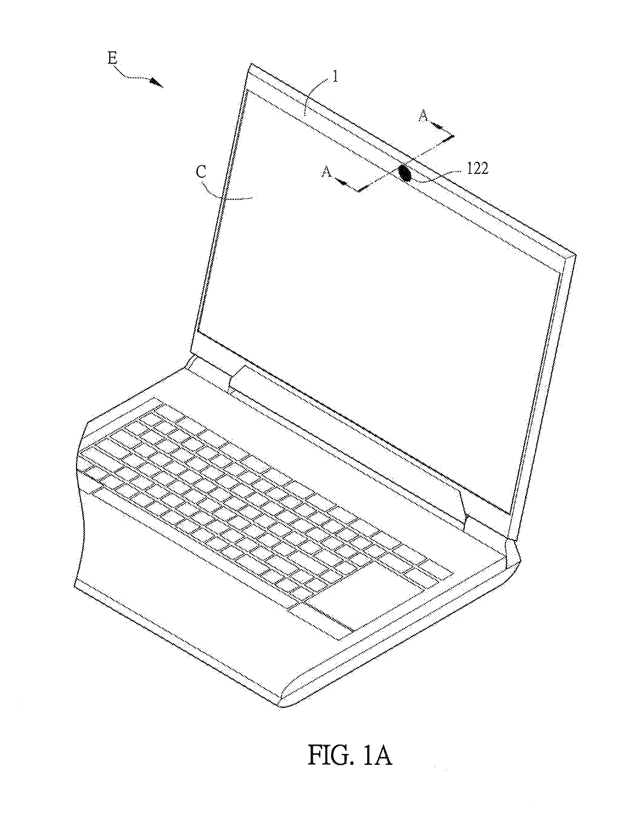
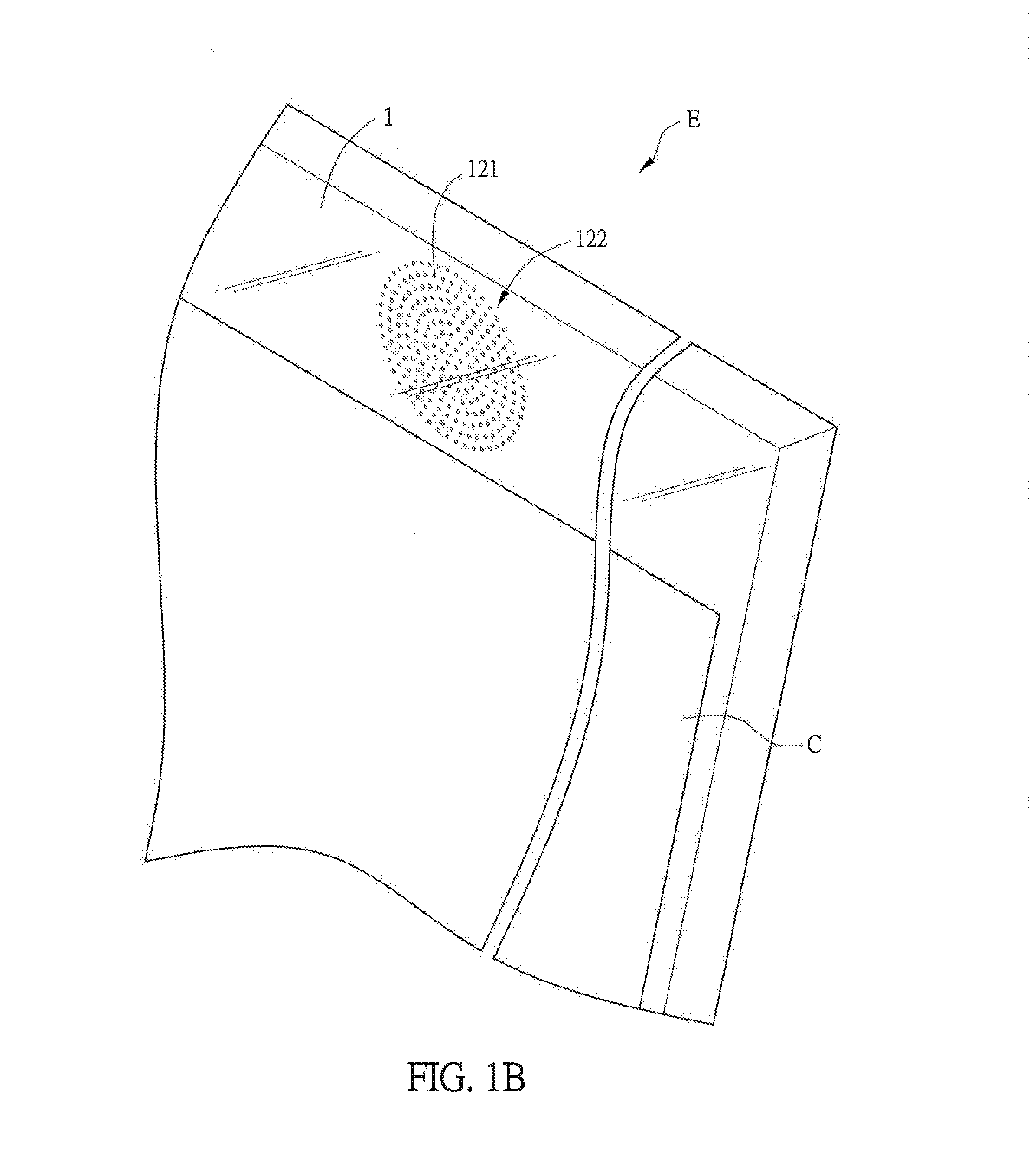
[0019]FIG. 1A is a schematic diagram showing an optical panel used in an electronic device in an embodiment. FIG. 1B is a partial enlarged drawing showing the optical panel in FIG. 1A. FIG. 2 is a schematic diagram showing the cross-section A-A of the optical panel in FIG. 1A. As shown in FIG. 1, an optical panel 1 is mainly used at an electronic device E. Please refer to the FIG. 1B and FIG. 2, the optical panel 1 includes a light transparent panel 11, a light shielding layer 12 and an optical element 13. The light transparent panel 11 may be but not limited to glass, acrylic or transparent film as long as it is a transparent material. The light shielding layer 12 is disposed on one surface of the light transparent panel 11 and includes a plurality of light transmission holes 121. The optical element 13 is disposed adjacent to the surface of the light transparent panel 11 with the light-shielding layer 12.
[0020]The light shielding layer 12 can make the light transparent panel 11 op...
PUM
 Abstract
Description
Claims
Application Information