Package structure of optical apparatus

a technology of optical apparatus and package structure, applied in the field of package structure, can solve the problems of not being able to effectively reduce the overall volume of the conventional proximity optical sensor b>100/b>, not being able to achieve the effect of reducing the overall volume and size of the package structur

Active Publication Date: 2013-12-12
PIXART IMAGING INC
View PDF25 Cites 25 Cited by
  • Summary
  • Abstract
  • Description
  • Claims
  • Application Information

AI Technical Summary

Benefits of technology

[0017]According to the above, the package structure of the optical apparatus of the present invention comprises a light sensing device which is a chip scale package (CSP) device, and it does not require the conventional wire bonding, so the overall volume and size of the package structure of the optical apparatus is reduced. In addition, the multilayer film disposed on the light sensing dev...

Problems solved by technology

Thus, it is not easy to reduce the size (e.g., the width W1) of the second accommodating space 134.
However, although the employment of the shielding structure 136 may effect...

Method used


Image

  • Package structure of optical apparatus
  • Package structure of optical apparatus
  • Package structure of optical apparatus

Examples


Embodiment Construction

[0028]The above and other technical details, features and effects of the invention will be will be better understood with regard to the detailed description of the embodiments below, with reference to the drawings. In the description, the words relate to directions such as “upper”, “on”, “above”, etc. are used to illustrate relative orientations in the drawings and should not be considered as limiting in any way.

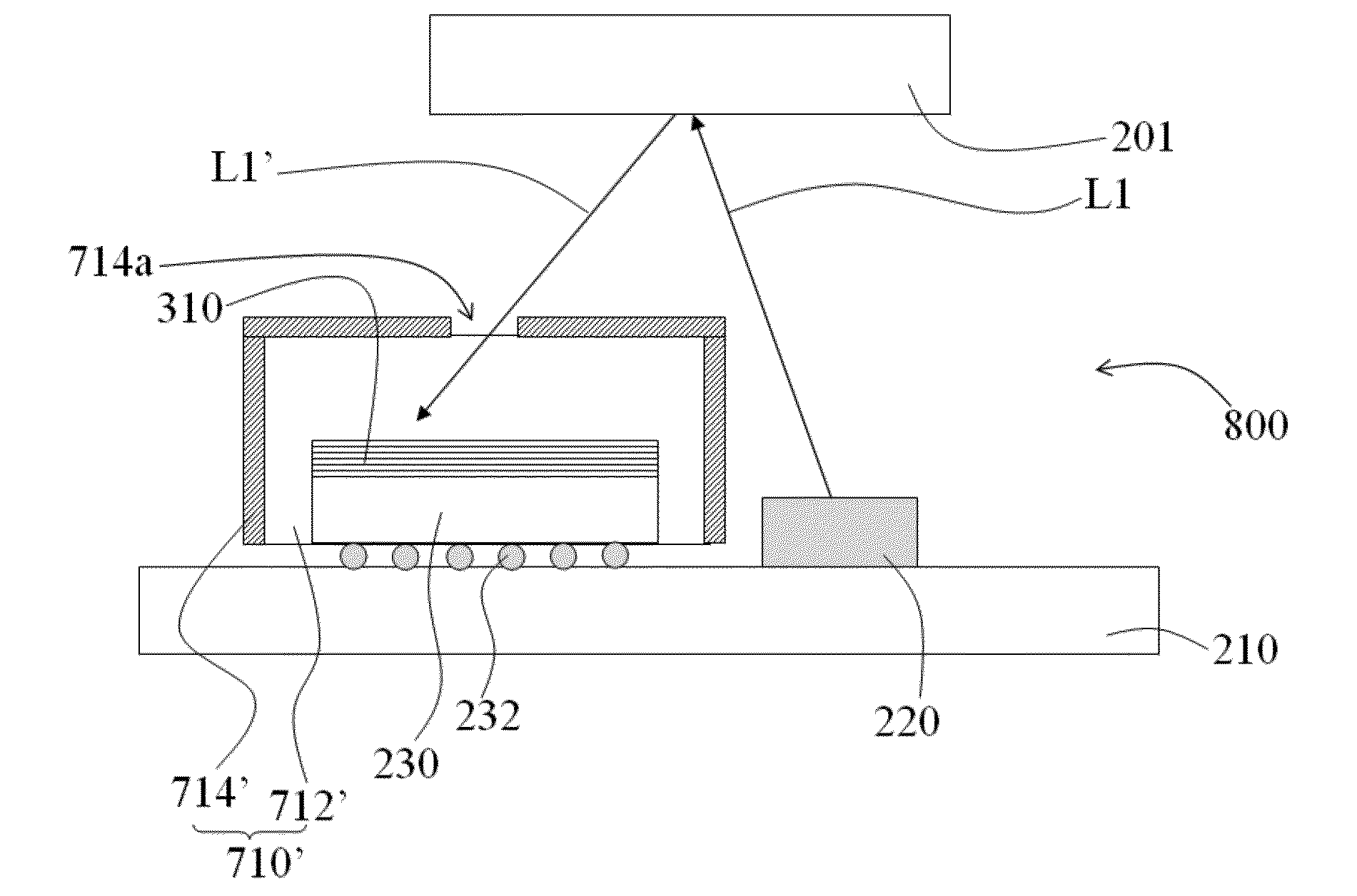
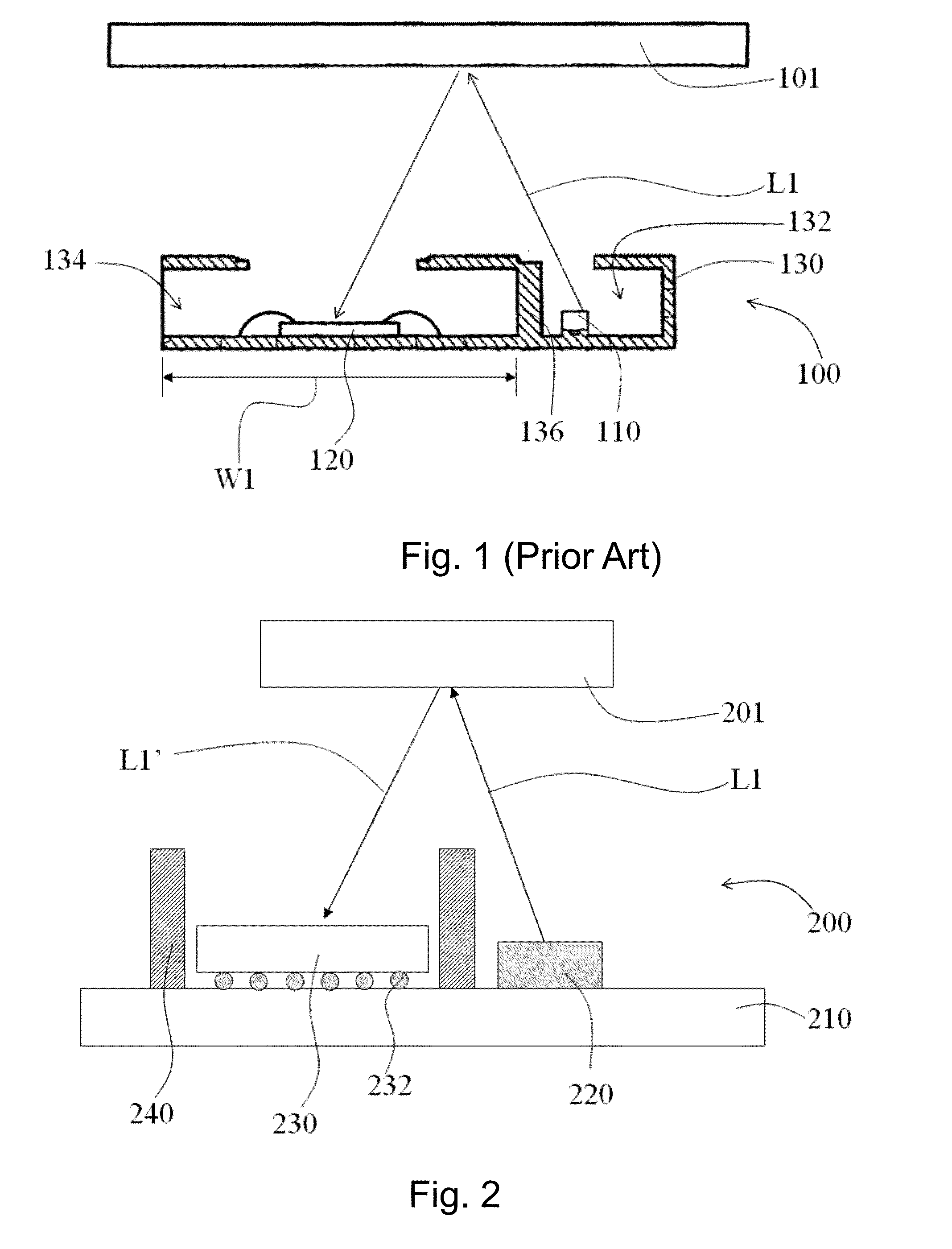
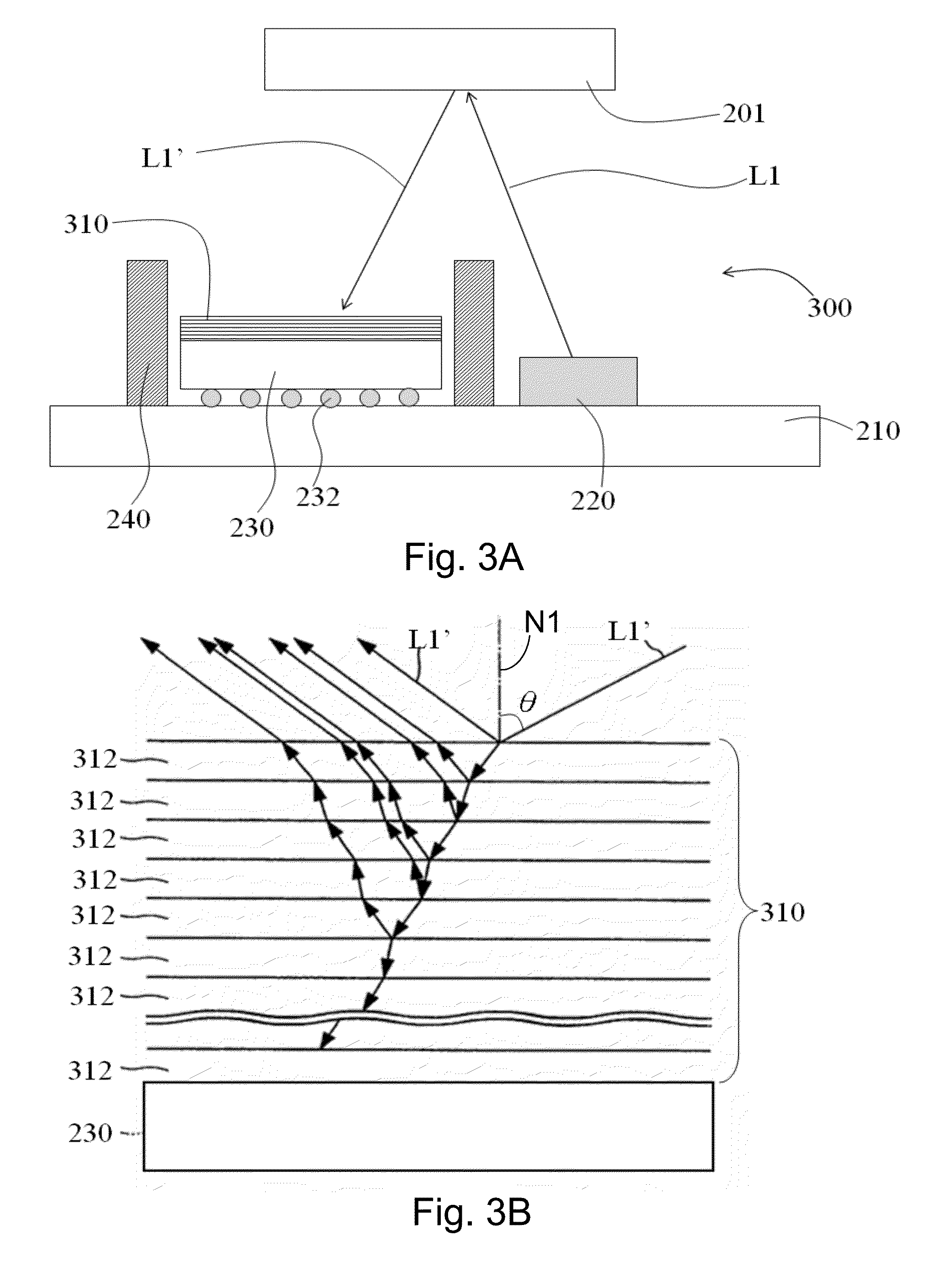
[0029]FIG. 2 shows a schematic view of a package structure of an optical apparatus according to an embodiment of the present invention. The package structure of the optical apparatus 200 of this embodiment is illustrated by taking an optical proximity sensor as an example. The package structure of the optical apparatus 200 comprises a substrate 210, alight emitting device 220, a light sensing device 230, and a light barrier member 240. The light emitting device 220 is disposed on the substrate 210 and electrically connected to the substrate 210. The light emitting device 220...


PUM


Abstract

The present invention provides a package structure of an optical apparatus which includes a substrate, a light emitting device, a light sensing device, and a light barrier member. The light emitting device is disposed on the substrate and electrically connected to the substrate. The light emitting device is for emitting light. The light sensing device is disposed on the substrate and is a chip scale package (CSP) device. The light sensing device is for receiving light reflected by an object. The light barrier member is disposed around a periphery of the light sensing device.

Description

CROSS REFERENCE[0001]The present invention claims priority to TW 101120195, filed on Jun. 6, 2012.BACKGROUND OF THE INVENTION[0002]1. Field of Invention[0003]The present invention relates to a package structure; particularly, it relates to such package structure for an optical apparatus.[0004]2. Description of Related Art[0005]FIG. 1 shows a cross-sectional view of the package structure of a conventional optical proximity sensor. Please refer to FIG. 1. The conventional optical proximity sensor 100 comprises a light source 110, a light detector 120 and a package housing 130. The package housing 130 includes a first accommodating space 132 and a second accommodating space 134. The light source 110 is disposed in the first accommodating space 132. The light detector 120 is disposed in the second accommodating space 134. In this conventional optical proximity sensor 100, when an object 101 approaches the conventional optical proximity sensor 100, the light beam L1 emitted from the ligh...

Claims


Application Information

Patent Timeline
IPC IPC(8): G01V8/12G01S17/04
CPCG01V8/12H01L31/02162H01L2224/16225G01S7/4813G01S17/04H01L31/167H01L31/0203H01L31/02005H01L31/02164H01L31/143
Inventor HSU, EN-FENGCHEN, NIEN-TSE
Owner PIXART IMAGING INC
Why Eureka
Try Eureka