Mask for deposition and method for manufacturing organic light emitting diode display using the same

a technology of light-emitting diodes and masks, which is applied in the direction of vacuum evaporation coatings, solid-state devices, coatings, etc., can solve the problems of weak bridge portion of the mask supporting the portion between the slots, easy to break, and difficult to manufacture a deposition mask with a high resolution of more than 300 ppi (pixels per inch), so as to reduce the deposition margin of organic materials. , the effect of high resolution

Active Publication Date: 2013-12-19
SAMSUNG DISPLAY CO LTD
View PDF28 Cites 27 Cited by
  • Summary
  • Abstract
  • Description
  • Claims
  • Application Information

AI Technical Summary

Benefits of technology

[0013]Embodiments of the present invention provide a deposition mask realizing high resolution by reducing a depos

Problems solved by technology

However, if the interval within the mask pattern is decreased, a bridge portion of the mask supporting a portion between the slots becomes weak and

Method used


Image

  • Mask for deposition and method for manufacturing organic light emitting diode display using the same
  • Mask for deposition and method for manufacturing organic light emitting diode display using the same
  • Mask for deposition and method for manufacturing organic light emitting diode display using the same

Examples


Embodiment Construction

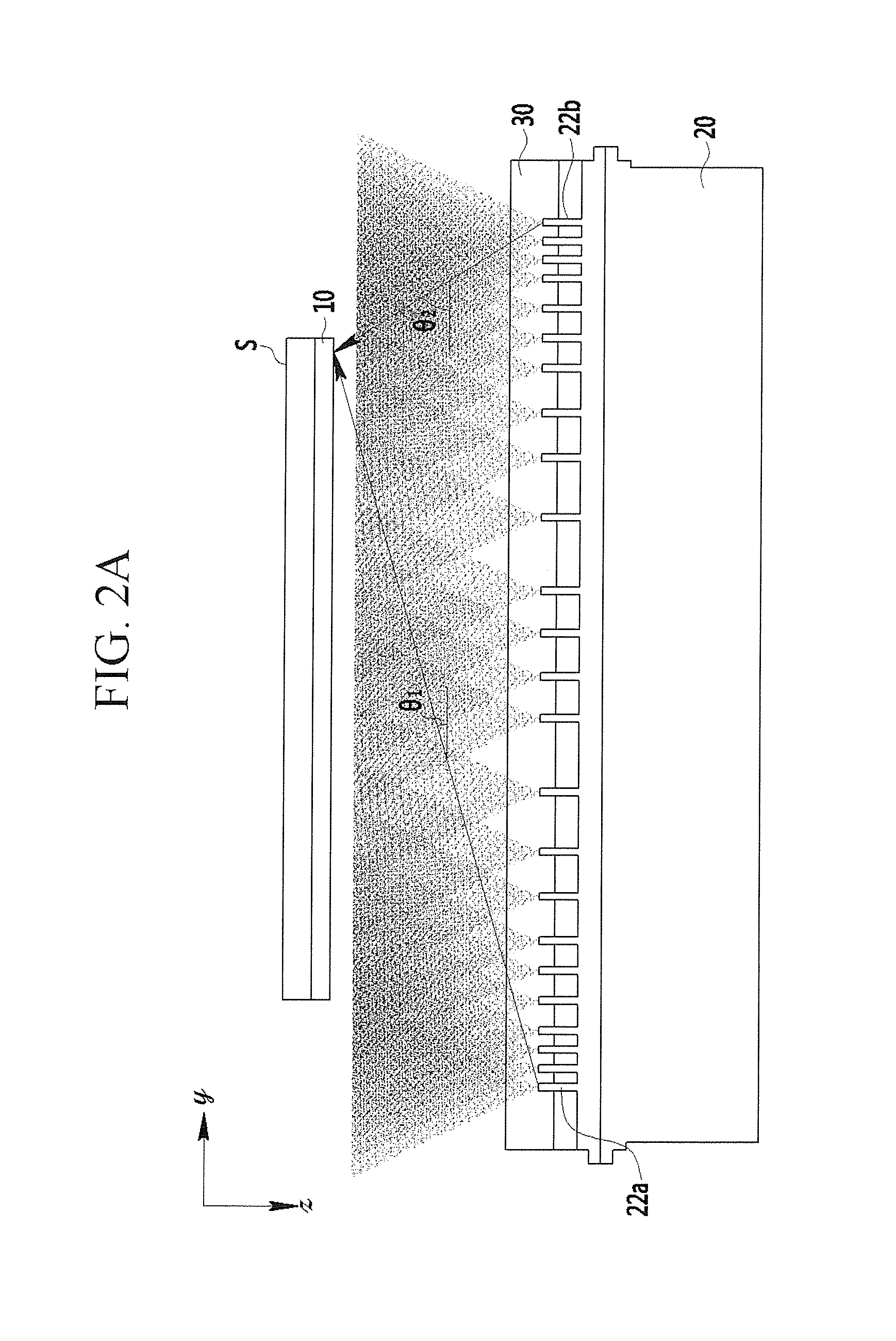
[0034]A deposition mask and a method for manufacturing an organic light emitting diode (OLED) display according to embodiments of the present invention will be described with reference to the accompanying drawings. However, the present invention is not limited to the exemplary embodiments disclosed hereinafter, but may be implemented in various different forms. The exemplary embodiments herein merely complete the disclosure of the present invention and fully provide explanation of the invention to the ordinarily skilled person in the art. Like reference numerals refer to like elements.

[0035]In the drawings, the thickness of layers, films, panels, regions, etc., may be exaggerated for clarity. In the drawings, for better understanding and ease of description, the thicknesses of some layers and areas may be exaggerated. It will be understood that when an element such as a layer, film, region, or substrate is referred to as being “on” another element, it can be directly on the other el...


PUM

PropertyMeasurementUnit
Angleaaaaaaaaaa
Angleaaaaaaaaaa
Angleaaaaaaaaaa

Abstract

A deposition mask for forming an organic layer pattern of an organic light emitting diode (OLED) display includes a base member having a first surface facing a substrate of the OLED display, and a second surface facing a side opposite to the first surface, and including a plurality of openings passing through the first surface and the second surface for forming the organic layer pattern. The opening has a pair of first side walls and a pair of second side walls. Each side wall of the openings has an inclination surface inclined with respect to a thickness direction of the base member, and when measuring an inclination angle of the inclination surface with reference to the first surface of the base member, the inclination angle of the first side wall and the inclination angle of the second side wall are different from each other.

Description

CROSS-REFERENCE TO RELATED APPLICATION[0001]This application claims priority to and the benefit of Korean Patent Application No. 10-2012-0063224 filed in the Korean Intellectual Property Office on Jun. 13, 2012, the entire content of which is incorporated herein by reference.BACKGROUND[0002]1. Field[0003]The described technology relates generally to a mask for thin film deposition and a manufacturing method of an organic light emitting diode (OLED) display.[0004]2. Description of the Related Art[0005]An organic light emitting diode (OLED) display includes a hole injection electrode, an electron injection electrode, and an organic emission layer formed therebetween, and the display emits light as holes injected from an anode and electrons injected from a cathode are recombined to form excitons at the organic light emission layer. The organic light emitting diode (OLED) display device, having high quality properties such as low power consumption, high luminance, a wide viewing angle, ...

Claims


Application Information

Patent Timeline
IPC IPC(8): H01L51/56
CPCH01L51/56C23C14/042H10K71/166H10K71/00C23C14/04
Inventor LEELEE, CHOONG-HO
Owner SAMSUNG DISPLAY CO LTD
Why Eureka
Try Eureka