
Integrated circuit chip and memory device

Inactive Publication Date: 2013-12-19
SK HYNIX INC
View PDF5 Cites 12 Cited by
  • Summary
  • Abstract
  • Description
  • Claims
  • Application Information

AI Technical Summary

Benefits of technology

The present invention prevents abnormal operations caused by erroneous settings by only activating the highest priority setting when multiple functions have the same priority.

Problems solved by technology

Meanwhile, new functions are gradually added to the memory devices, resulting in an increase in the number of pins (or balls) in the memory devices.

Method used


Image

  • Integrated circuit chip and memory device
  • Integrated circuit chip and memory device
  • Integrated circuit chip and memory device

Examples


Embodiment Construction

[0018]Exemplary embodiments of the present invention will be described below in more detail with reference to the accompanying drawings. The present invention may, however, be embodied in different forms and should not be construed as limited to the embodiments set forth herein. Rather, these embodiments are provided so that this disclosure will be thorough and complete, and will fully convey the scope of the present invention to those skilled in the art. Throughout the disclosure, like reference numerals refer to like parts throughout the various figures and embodiments of the present invention. In this specification, a singular form may include a plural form as long as it is not specifically mentioned in a sentence.

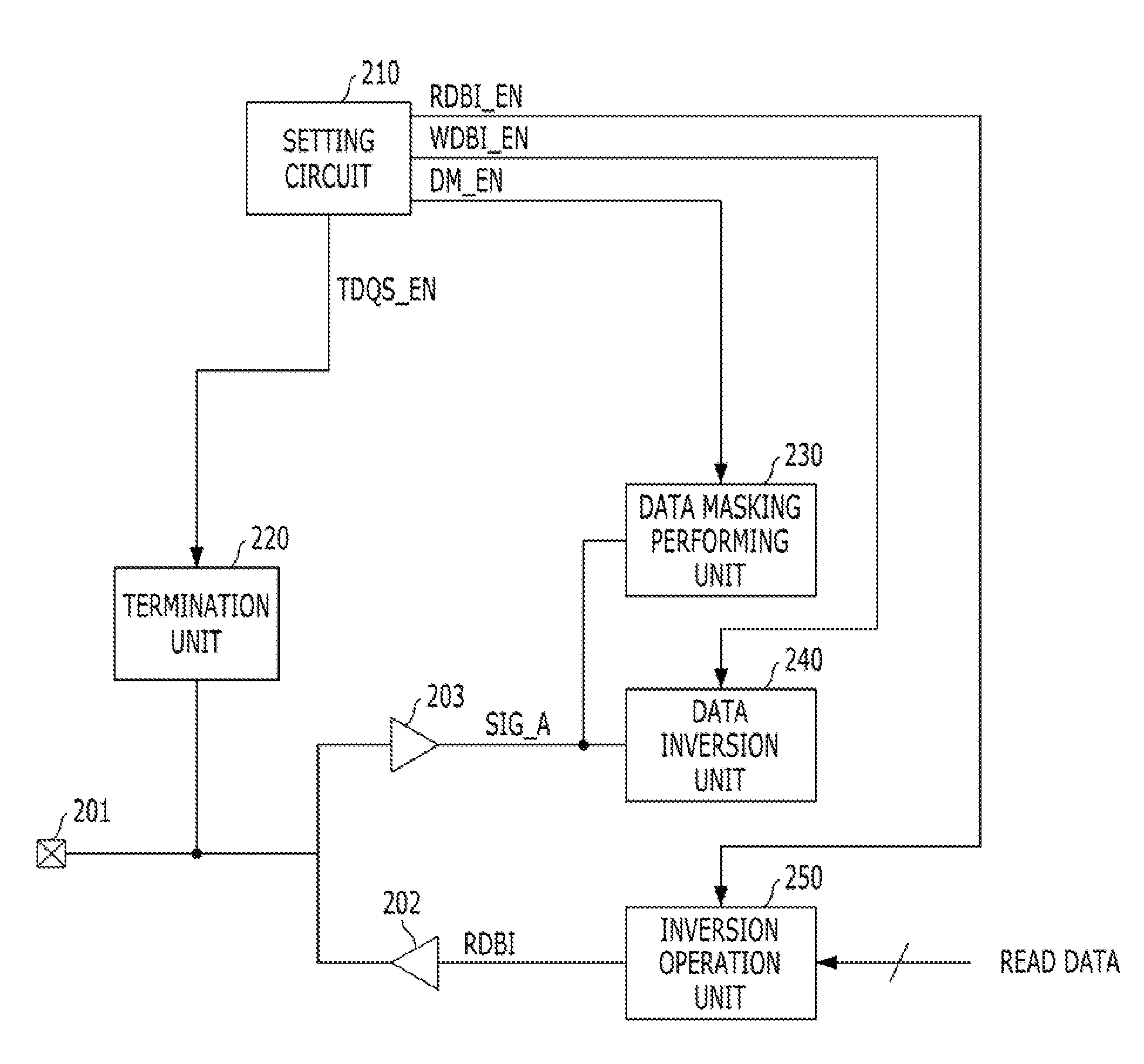
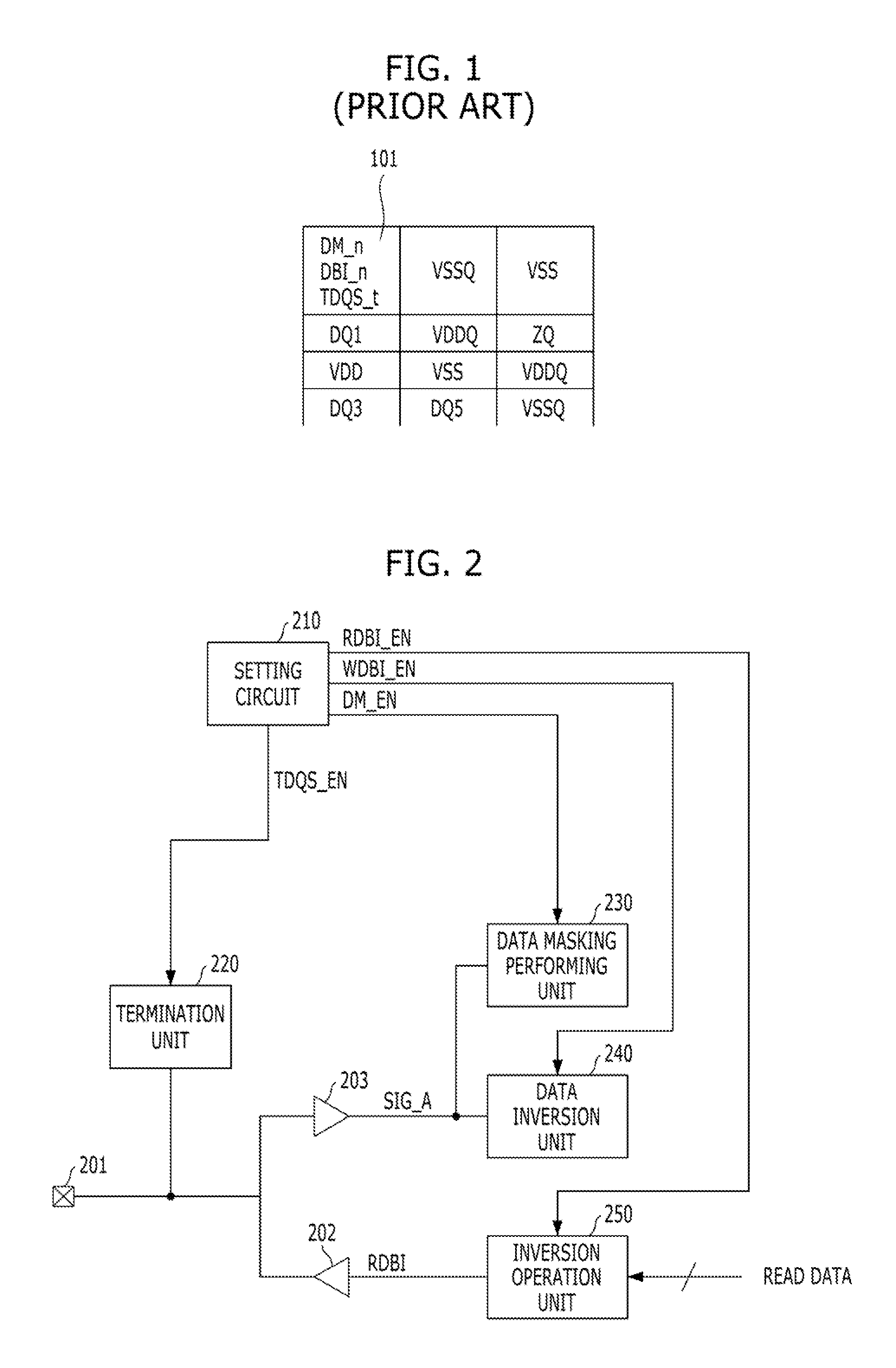
[0019]FIG. 2 is a block diagram of a memory device in accordance with an embodiment of the present invention.

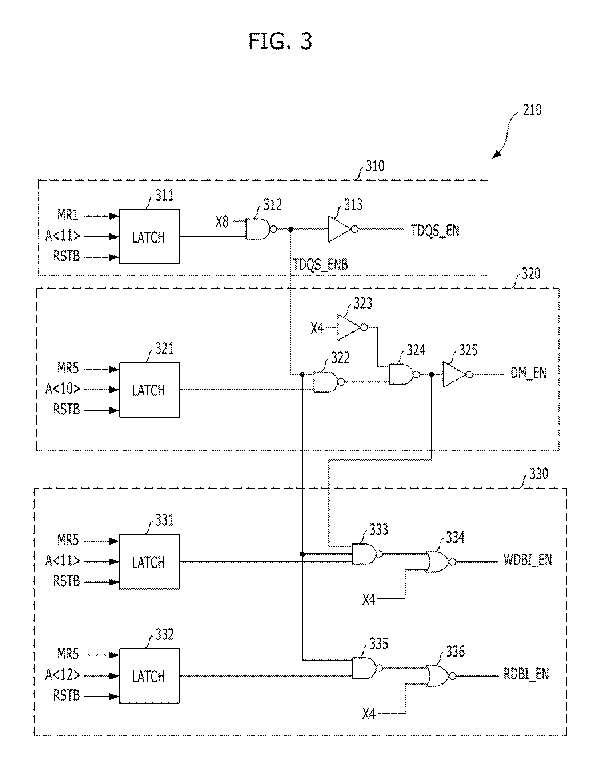
[0020]Referring to FIG. 2, the memory device includes a pad 201, to which a package ball (or pin) is connected, a setting circuit 210, a termination unit 220, a ...


PUM


Abstract

A memory device includes a pad that provides an interface with an exterior, a first setting unit that generates a termination setting signal for setting the pad for a purpose of termination data strobe using a first specific code of a mode register set operation, a second setting unit that generates a mask setting signal for setting the pad for a purpose of data mask using a second specific code of the mode register set operation, and a third setting unit that generates a write inversion setting signal for setting the pad for a purpose of write data bus inversion using third specific code of the mode register set operation. When a setting signal with a higher priority is activated, a setting signal with a lower priority is deactivated regardless of a value of the corresponding code.

Description

CROSS-REFERENCE TO RELATED APPLICATIONS[0001]The present application claims priority of Korean Patent Application No. 10-2012-0063265, filed on Jun. 13, 2012, which is incorporated herein by reference in its entirety.BACKGROUND[0002]1. Field[0003]Exemplary embodiments of the present invention relate to a memory device, and more particularly, to a technology for setting a pad of a memory device to perform various functions.[0004]2. Description of the Related Art[0005]In a memory field, there have been increasing demands for low power consumption and a high speed operation, and memory devices of new standards are continuously provided according to such demands. Meanwhile, new functions are gradually added to the memory devices, resulting in an increase in the number of pins (or balls) in the memory devices.[0006]FIG. 1 is a diagram illustrating a part of a package ball arrangement in a memory device.[0007]Referring to FIG. 1, in the case of balls VSSQ, VSS, VDD, and VDDQ for power sup...

Claims


Application Information

Patent Timeline
IPC IPC(8): G06F12/06
CPCG06F12/0646G11C7/1009G11C7/1045G11C7/10G11C7/22G11C7/24
Inventor OK, SUNG-HWAKU, KIE-BONGLEE, HYE-YOUNGYOO, SEJIN
Owner SK HYNIX INC
Learn More