

High-voltage output apparatus and image forming apparatus
a high-voltage output and image forming technology, which is applied in the direction of electrographic process apparatus, instruments, corona discharge, etc., can solve the problem that the control method based on the information in the memory of the cartridge has a limit in correcting the variations of the voltage difference between vdc and vl
- Summary
- Abstract
- Description
- Claims
- Application Information
AI Technical Summary
Benefits of technology
Problems solved by technology
Method used
Image


Examples
embodiment 1
[0040]In embodiment 1, focusing on this characteristic, a potential difference necessary for a discharge to a drum and a surface potential on the drum are detected, and based on the detection results, the light amount of a laser beam is variably set.
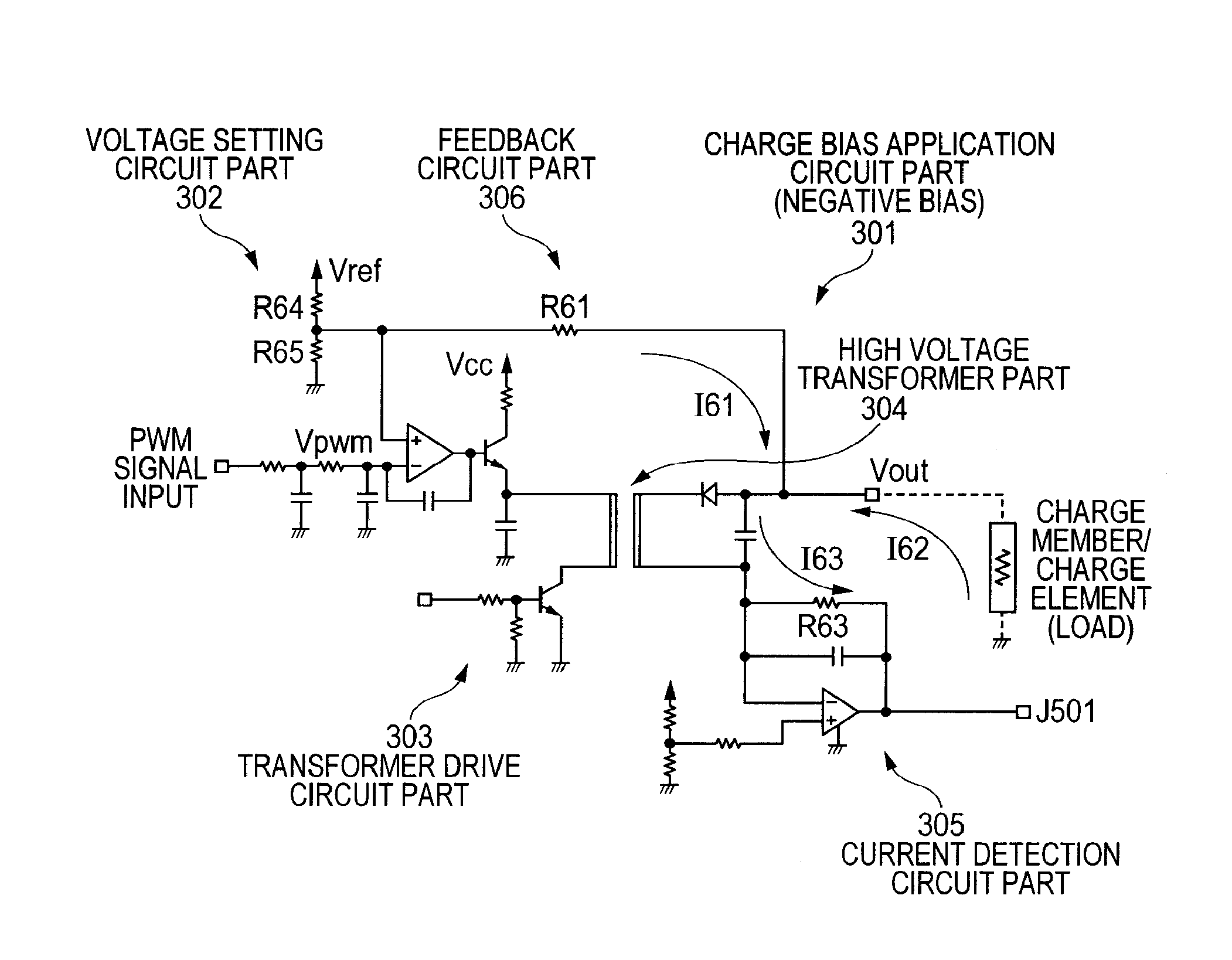
[0041]FIG. 3 is a schematic diagram of an image forming apparatus according to embodiment 1. The image forming apparatus includes a drum 201, a charge roller 202 (hereinafter referred to as “C roller” or “charge member”), a developing roller 203 (hereinafter also referred to as “developing sleeve”), a transfer roller 204, a charge bias application circuit 206, and a light source 205 that emits a laser beam. A series of control for image formation is started after charge (potential) remaining on the drum 201 is eliminated by an alternate voltage (hereinafter referred to as “AC bias”) applied from the charge bias application circuit 206.
[0042]FIG. 4 illustrates a schematic configuration of a charge bias application circuit 301 (voltage app...
embodiment 2
[0061]Next, control in embodiment 2 will be described with reference to the flowcharts in FIGS. 9A and 9B and the potential diagrams in FIGS. 10A, 10B, 10C and 10D.
[0062]First, after power-on or receipt of a print command (S400), an non-image region on the photosensitive drum, an element to be charged, which is being rotated by means of an operation for, e.g., a multiple-pre-rotation process or a pre-rotation process (S401), a residual potential on the drum is neutralized by means of an AC bias (S402). Subsequently, a predetermined negative bias (a set value of a PWM signal: PWM(1)) is applied to charge a surface of the drum with a negative potential (S403).
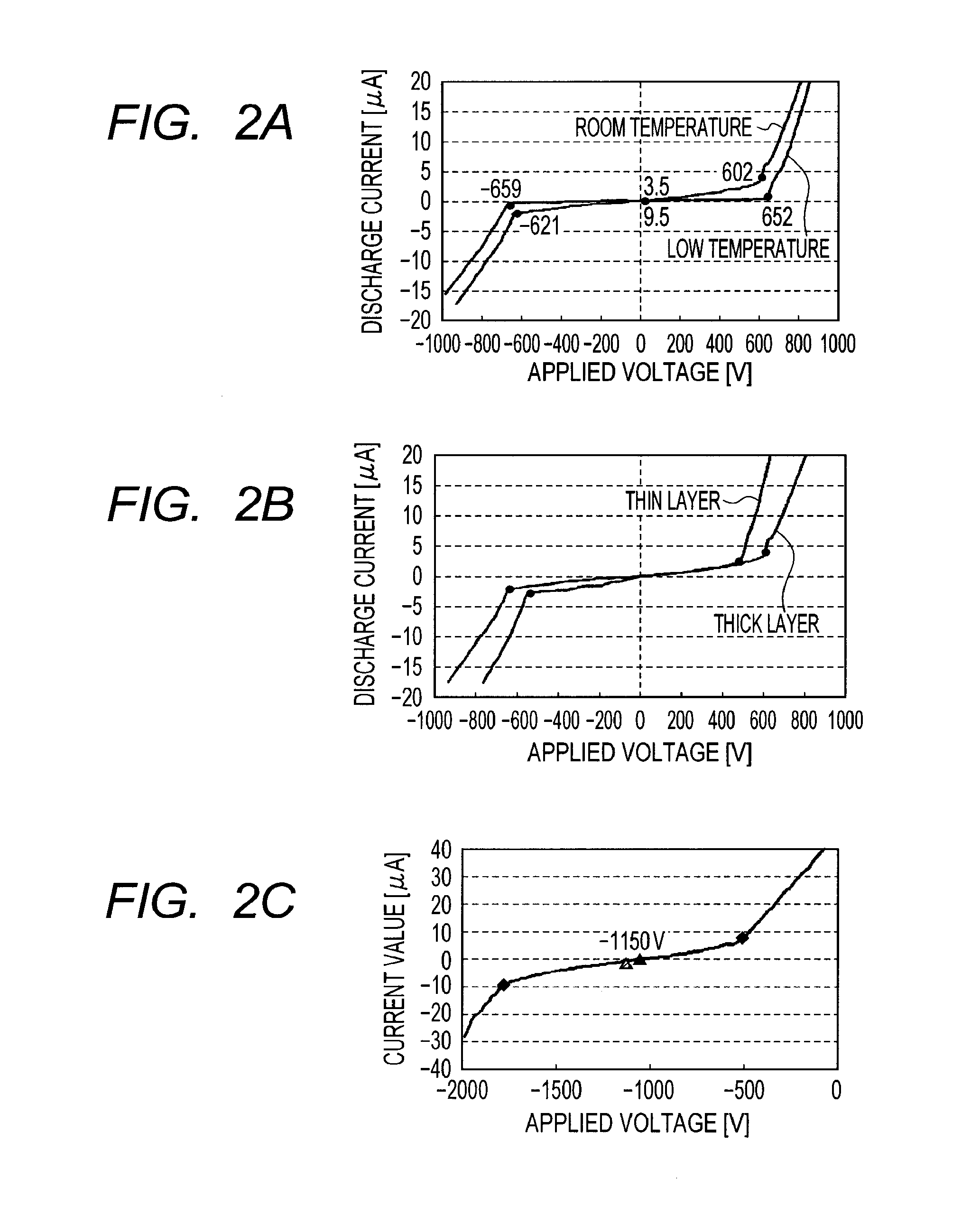
[0063]In such state, using a charge bias application circuit, a bias (DC bias) with the potential of the drum, which has been charged with the predetermined negative potential, as its center is applied to the drum. First, the absolute value of the voltage is gradually decreased (S404). The current I63 with a current value that is...
PUM
 Abstract
Description
Claims
Application Information