Eureka AIR delivers breakthrough ideas for toughest innovation challenges, trusted by R&D personnel around the world.

Method for creating and preserving alignment marks for aligning mask layers in integrated circuit manufacture

a technology of integrated circuits and alignment marks, which is applied in the direction of instruments, semiconductor devices, photomechanical treatment, etc., can solve the problems of increasing costs, increasing costs, and requiring additional equipmen

Inactive Publication Date: 2001-07-17
NEWPORT FAB
View PDF16 Cites 90 Cited by
  • Summary
  • Abstract
  • Description
  • Claims
  • Application Information

AI Technical Summary

Benefits of technology

It is still another object of the present invention to provide a method for producing and preserving alignment marks for forming integrated circuits which does not result in added wafer cost or loss in throughput and cycle time.

Problems solved by technology

Without automatic alignment, an operator would have to individually align several hundred die on a wafer at a productive rate, which is nearly impossible.
Nevertheless, there are many cases in which the alignment of non-successive layers is necessary where the intervening layer is opaque.
Further, alignment marks may be effected by subsequent processing of the pattern transferred to the wafer surface thereby rendering it more difficult to be observed for alignment.
This results in increased costs and the need for additional equipment.
The repeated steps required for the metal removal process impacts cycle time and results in an increase in costs of up to $27 or more per wafer per metal layer that is removed.
Due to the use of extended tabs used in this process, metal shadowing causes die loss at the shadow tab sites and the dies located near the shadow tab sites.
The greater the number of tabs used, the greater the number of die losses that are incurred.
In addition to the die loss problem, the shadow tab process also creates metal sticking problems in the metal deposition systems which require more frequent preventative maintenance during wafer processing.
In addition, the die loss and increased preventative maintenance results in equipment downtime.
Unfortunately, neither the metal alignment mark generation in Yu nor the alignment mark recovery in Chang et al. address the problems with non-visible alignment marks, non-symmetrical alignment marks, and damaged alignment marks which can result from planarization using chemical mechanical polishing.

Method used


Image

  • Method for creating and preserving alignment marks for aligning mask layers in integrated circuit manufacture
  • Method for creating and preserving alignment marks for aligning mask layers in integrated circuit manufacture
  • Method for creating and preserving alignment marks for aligning mask layers in integrated circuit manufacture

Examples


Embodiment Construction

The present invention may be described herein in terms of various processing steps. It should be appreciated by those skilled in the art that such processing steps may be realized by any number and combination of various conventional techniques and equipment for carrying out those techniques. It should also be appreciated that the particular implementations and process steps shown and described herein are illustrative of the invention and its best mode, and are not intended to otherwise limit the scope of the present invention in any way.

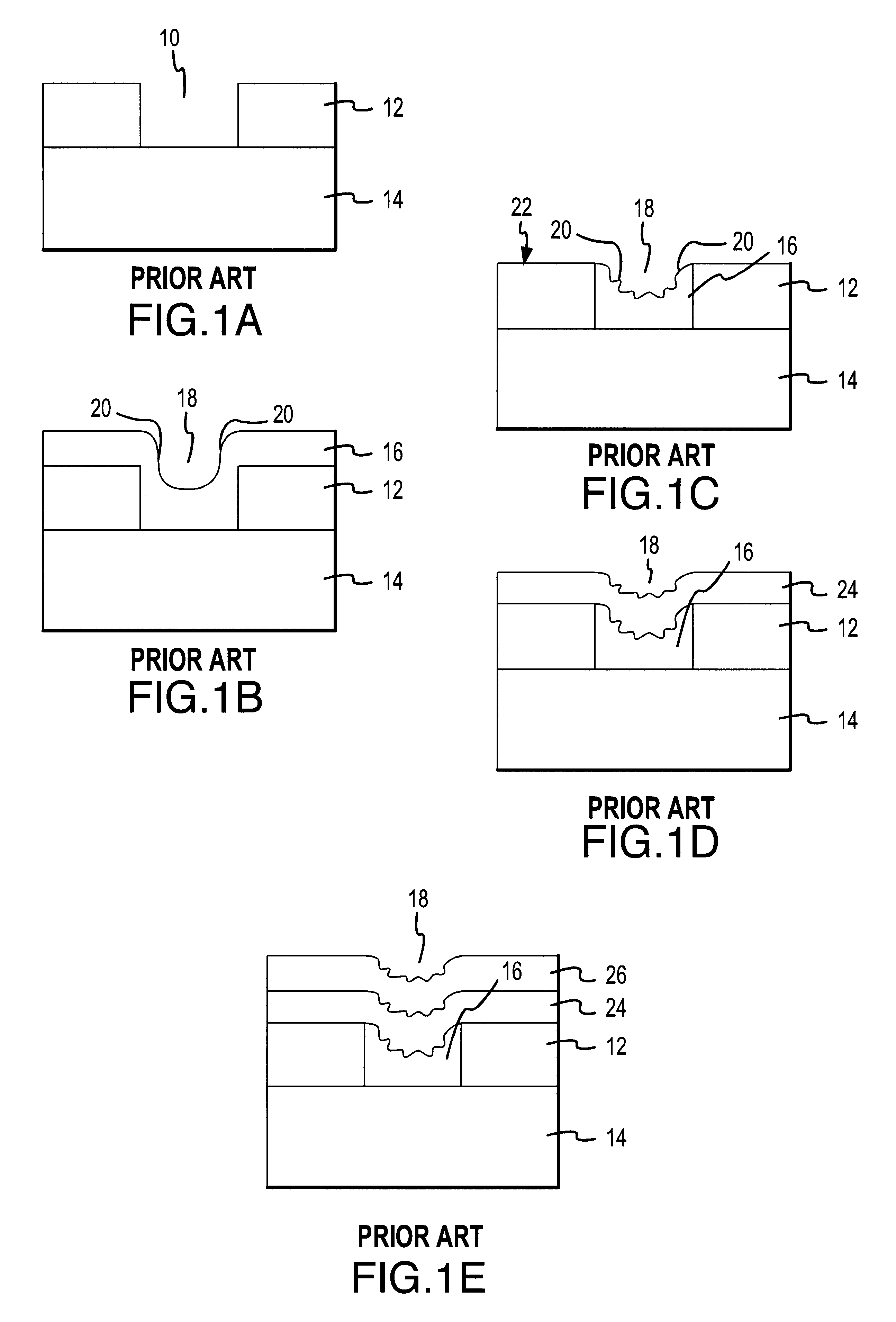
FIGS. 1A-1E refer to various stages in the prior art creation of an alignment mark used with conventional chemical mechanical processing (CMP). For example, as illustrated in FIG. 1A, a trench 10 is etched in a dielectric layer 12 which has been deposited on the surface of a wafer substrate 14, such as silicon. The trench 10 serves as a mold for an alignment mark. In FIG. 1B, a first metal layer 16, such as tungsten, for example, is conformably depo...


PUM

PropertyMeasurementUnit
dimensionsaaaaaaaaaa
sizeaaaaaaaaaa
energyaaaaaaaaaa

Abstract

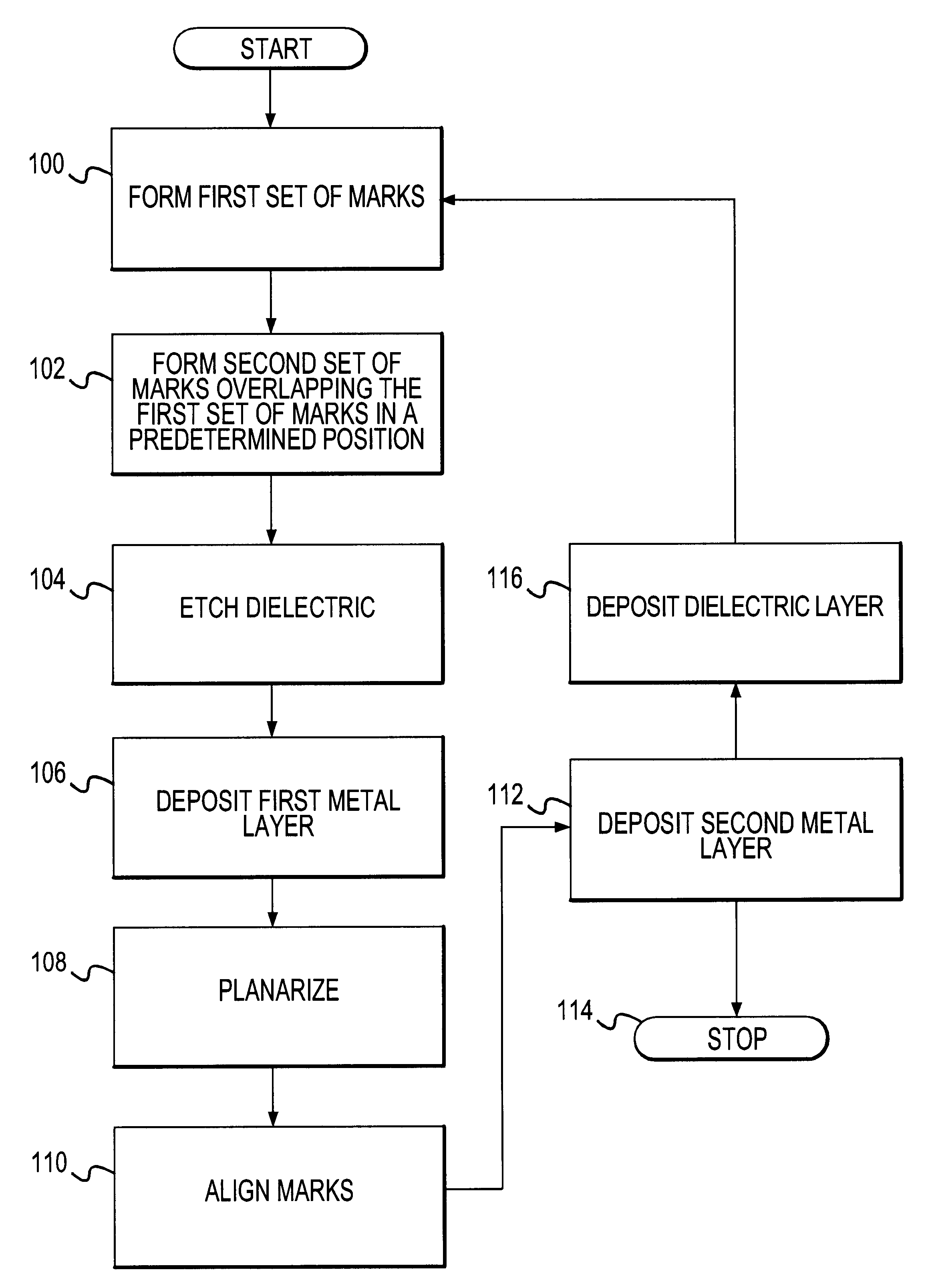
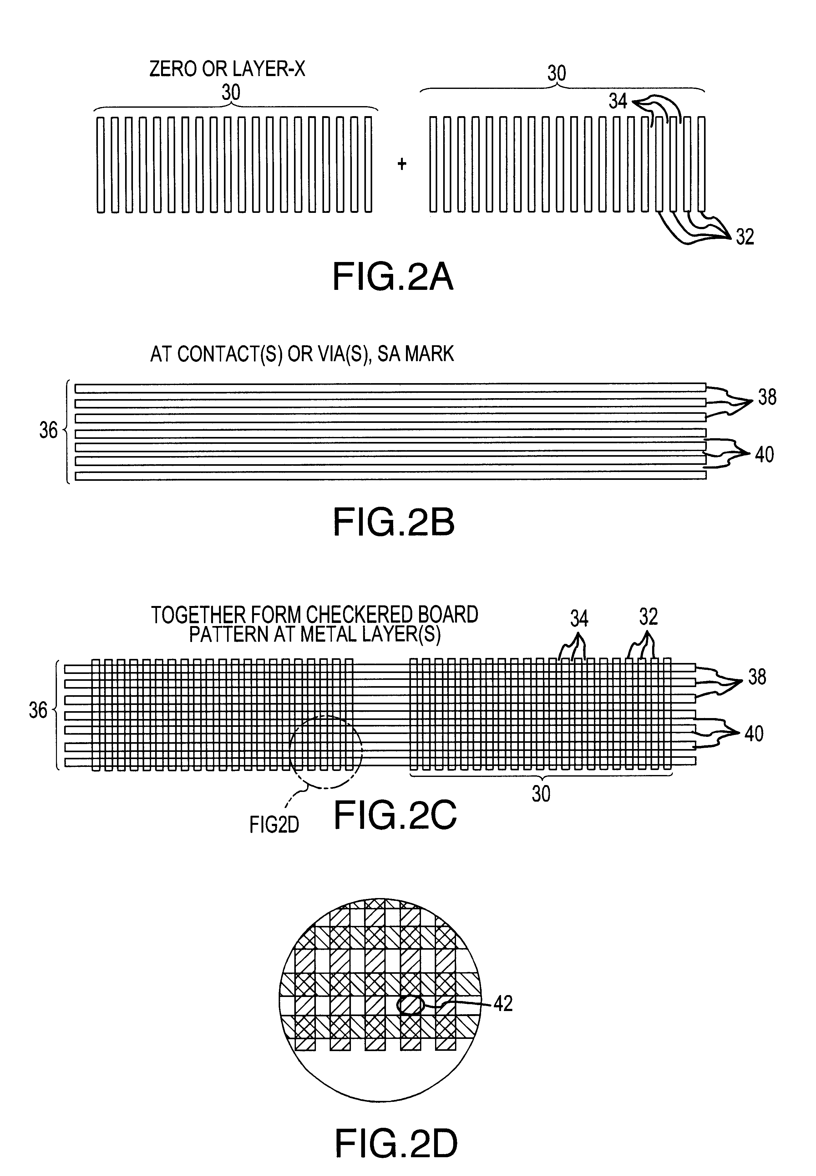
A method for creating and preserving alignment marks used for aligning mask layers in integrated circuit formation including the steps of creating a first set of marks within a reference layer to form a basic alignment mark, creating a second set of marks overlapping the first set of marks and positioned perpendicular to the first set of marks in the same reference layer to form a preservation pattern, and etching the reference layer to form a substantially checkerboard-type pattern where portions of the first set of marks are recessed within a thickness of the reference layer. After creating the checkerboard-type pattern formed from the first and second marks, a first metal a layer may be deposited to fill in any recesses contained within the pattern. CMP follows without damaging the segmented portions of the first set of marks which lie recessed within a thickness of the reference layer. Finally, the preserved portions of the first set of marks are aligned with pattern marks for a second metal layer.

Description

BACKGROUND OF THE INVENTIONThe present invention relates generally to a method for creating metal alignment marks in the manufacture of semiconductor integrated circuits. More particularly, the present invention relates to a method in which two layers of marks are positioned in perpendicular direction to one another in order to create alignment marks for properly aligning mask layers in the formation of integrated circuits where the alignment marks are preserved after chemical mechanical polishing processes utilized during the formation of an integrated circuit. The metal alignment mark creation of the present invention does not require removal of metals from the alignment marks in order to see the alignment marks for proper aligning of mask layers.Microchip fabrication involves a series of processes such as layering, patterning and doping to create integrated circuits and semiconductor devices in and on a semiconductor wafer surface. As opposed to "non-integrated" circuits in which...

Claims


Application Information

Patent Timeline
Patent Type & Authority Patents(United States)
IPC IPC(8): G03F9/00H01L23/544
CPCG03F9/708G03F9/7084H01L23/544H01L2223/54453H01L2223/54426H01L2924/0002H01L2924/00
Inventor SO, DANIEL M.
Owner NEWPORT FAB
Why Eureka
Eureka Blog
Learn More