Device and method for manufacturing a semiconductor wafer

a semiconductor and manufacturing method technology, applied in semiconductor/solid-state device testing/measurement, program control, instruments, etc., can solve the problem of not being able to cancel out the variation in flatness, and achieve the effect of improving the surface profile of the manufactured semiconductor wafer

Active Publication Date: 2012-06-12
SUMCO TECHXIV
View PDF9 Cites 97 Cited by
  • Summary
  • Abstract
  • Description
  • Claims
  • Application Information

AI Technical Summary

Benefits of technology

[0011]With this semiconductor wafer manufacturing device, before the actual processing of a substrate wafer, the anticipated surface shapes of the manufactured wafers which would be obtained if that substrate wafer were to be processed under each of a plurality of different sets of processing conditions are predicted, and, on the basis of these predictions, one set of processing conditions among the plurality of sets of processing conditions can be selected which satisfies some demand. And the actual processing is performed under these selected processing conditions. Accordingly, it is possible to produce a manufactured wafer which has a satisfactory surface shape over its entire area.
[0015]By doing this, it is possible reliably to manufacture a manufactured wafer which satisfies a predetermined surface shape specification.
[0019]According to a preferred embodiment of the present invention, the profile of the surface of a manufactured semiconductor wafer is improved over substantially its entire area.

Problems solved by technology

However, since it is difficult to obtain an ideal state for both of these, an effective method has been to combine the surface shape of the substrate wafer with a layer thickness profile which is matched thereto, as described in Patent Reference #1.
For example, if the characteristics of the shape of the substrate wafers are determined by lot units, then it is not possible to cancel out variations in flatness due to differences in the shapes of different wafers within the same lot.

Method used


Image

  • Device and method for manufacturing a semiconductor wafer
  • Device and method for manufacturing a semiconductor wafer
  • Device and method for manufacturing a semiconductor wafer

Examples


Embodiment Construction

[0031]A semiconductor wafer manufacturing device according to an embodiment of the present invention will now be explained with reference to the drawings.

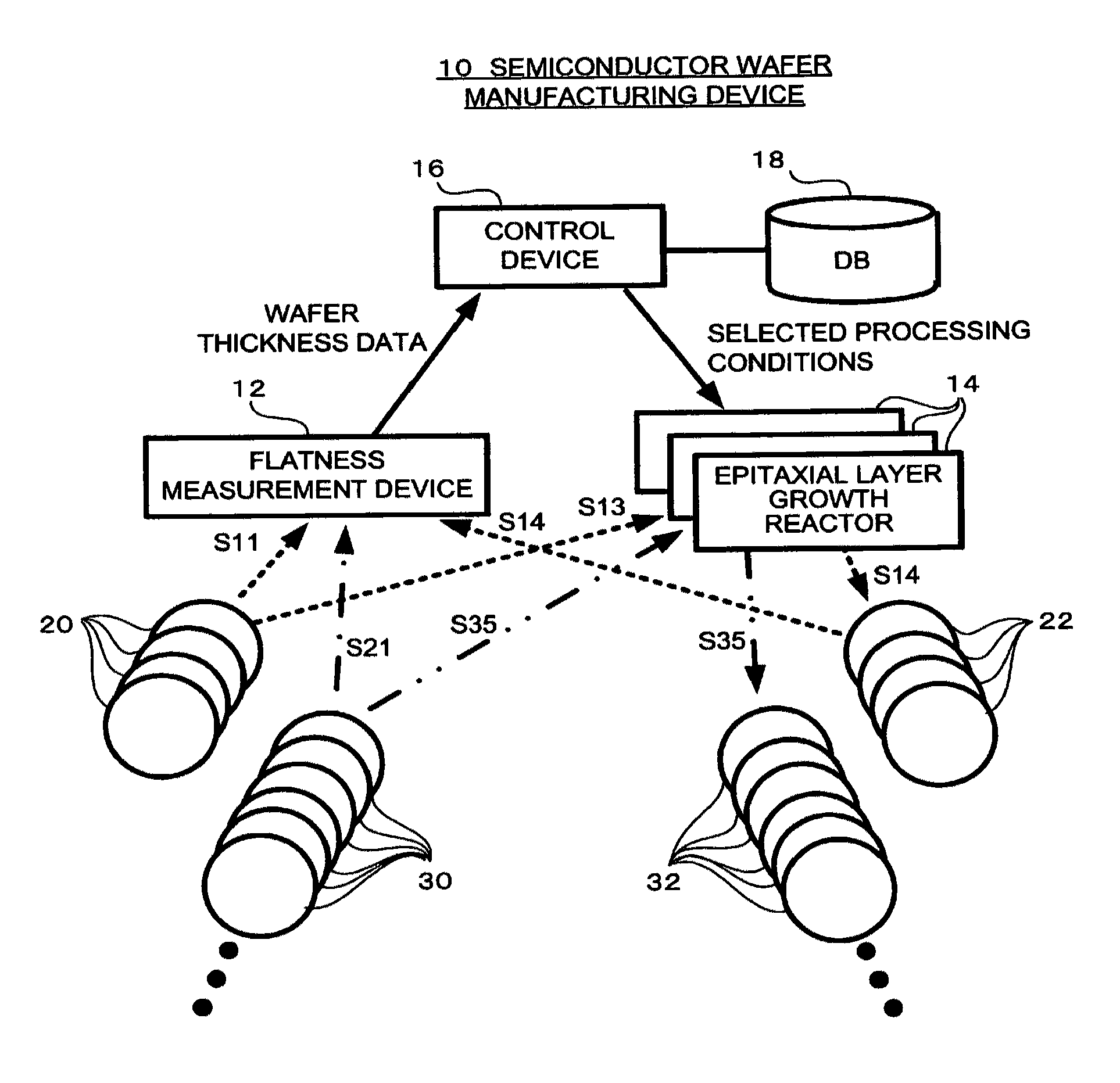
[0032]FIG. 1 shows the overall structure of a semiconductor wafer manufacturing device according to an embodiment of the present invention.

[0033]As shown in FIG. 1, this semiconductor wafer manufacturing device 10 comprises a flatness measurement device 12, one or more epitaxial layer growth reactors 14, 14, and a control device 16. The flatness measurement device 12 is a device for measuring the surface shape of a semiconductor wafer which is loaded thereinto—in this embodiment, its thickness profile. The epitaxial layer growth reactors 14 are devices for growing epitaxial layers upon the front surfaces of semiconductor wafers which are loaded thereinto. The control device 16 is a device for acquiring the thickness profiles of the semiconductor wafers as measured by the flatness measurement device 12, and for controlling the epita...


PUM

PropertyMeasurementUnit
diameteraaaaaaaaaa
diameteraaaaaaaaaa
areaaaaaaaaaaa

Abstract

In order to manufacture an epitaxial wafer having satisfactory flatness over its entire surface, epitaxial layers are experimentally grown upon actual wafer samples under various different layer formation conditions, the thickness profiles are measured over the entire surfaces of these wafers before and after growth of the layers, and, from the differences thereof, layer thickness profiles over the entire areas of the epitaxial layers under the various different layer formation conditions are ascertained and stored. Thereafter, the thickness profile of a substrate wafer is measured over its entire area, this is added to each of the layer thickness profiles under the various different layer formation conditions which have been stored, and the planarities of the manufactured wafers which would be manufactured under these various different layer formation conditions are predicted. And one set of processing conditions is selected which is predicted to satisfy a required flatness specification, and an epitaxial layer is actually grown upon the substrate wafer under these processing conditions.

Description

CROSS REFERENCE TO RELATED APPLICATIONS[0001]This application relates to and claims priority from Japanese Patent Application No. 2008-116166 filed on Apr. 25, 2008, the entire disclosure of which is incorporated herein by reference.FIELD OF THE INVENTION[0002]The present invention generally relates to a device and method for manufacturing a semiconductor wafer, and in particular relates to a technique for enhancing the flatness of a wafer which is manufactured via a process such as growth of an epitaxial layer or surface etching or the like.BACKGROUND OF THE INVENTION[0003]An example will be taken of manufacture of an epitaxial wafer by growing an epitaxial layer upon a substrate wafer. The flatness of the resulting epitaxial wafer may be determined by adding the thickness of the epitaxial layer to the shape of the surface of the substrate wafer. If there are variations in the flatness of the substrate wafer and for the thickness distribution of the epitaxial layer, then variations...

Claims


Application Information

Patent Timeline
Patent Type & Authority Patents(United States)
IPC IPC(8): B05C11/00H01L21/66B24B49/02C23F1/08
CPCH01L22/12H01L22/20G05B2219/37224G05B2219/37398
Inventor KUROSAWA, YOSHIAKI
Owner SUMCO TECHXIV
Why Eureka
Try Eureka