Method, apparatus and system for a per-dram addressability mode

a per-dram addressability and memory technology, applied in the direction of digital storage, instruments, computing, etc., can solve the problems of limited opportunities to provide more precision in such configuration, memory systems become increasingly sensitive to operational inefficiencies,

Active Publication Date: 2013-12-26
INTEL CORP
View PDF5 Cites 22 Cited by
  • Summary
  • Abstract
  • Description
  • Claims
  • Application Information

AI Technical Summary

Problems solved by technology

As the design and fabrication of memory system circuit logic continues to improve, memory systems become increasingly sensitive to operational inefficiencies.
However, the opportunities to provide more precision in such configuration are limited in memory rank applications.

Method used


Image

  • Method, apparatus and system for a per-dram addressability mode
  • Method, apparatus and system for a per-dram addressability mode
  • Method, apparatus and system for a per-dram addressability mode

Examples


Embodiment Construction

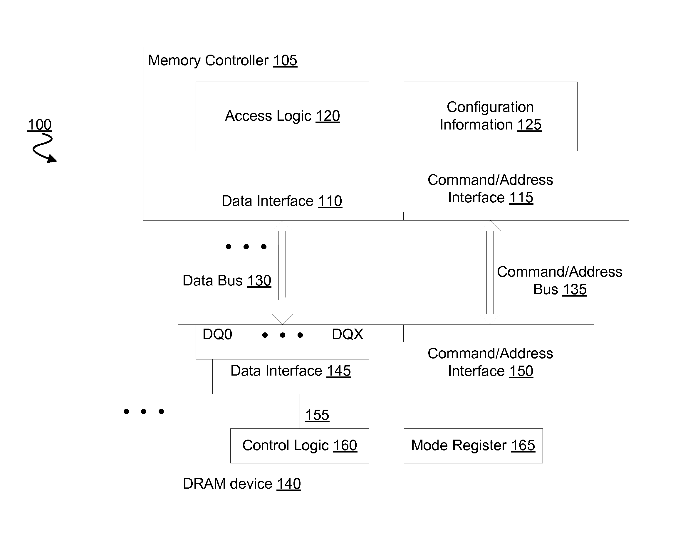
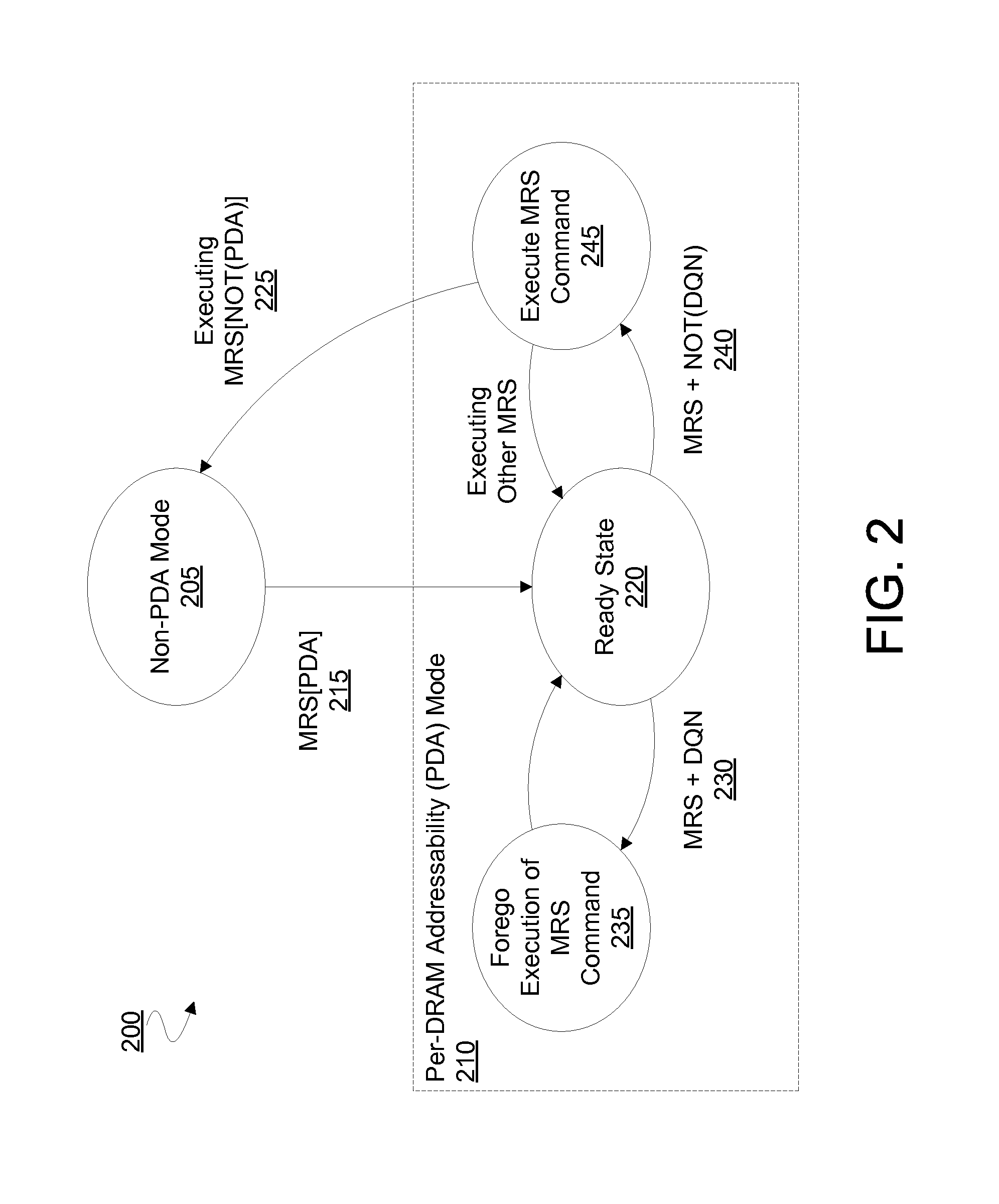
[0017]Embodiments variously provide for a per-DRAM addressability (PDA) mode of a DRAM device. While a PDA mode is enabled on a DRAM device, the device may be independently programmed by a memory controller on a device-specific basis—e.g. independent of any programming of one or more other memory devices of a rank which includes that DRAM device. Such programming may, for example, include setting one or more Mode Register Values of the DRAM device—e.g. to configure a reference voltage (Vref) value, an on-die termination (ODT) value and / or the like. Before entering PDA mode, a DRAM device may require write leveling, although certain embodiments are not limited in this regard.

[0018]The most recent draft of the DDR4 specification of the Joint Electron Devices Engineering Council (JEDEC) allows for inclusion of device-specific programmability in a rank of DRAM devices. While a DRAM device has a PDA mode enabled, execution of one or more mode register set (MRS) commands may be qualified ...


PUM


Abstract

Techniques and mechanisms for programming an operation mode of a dynamic random access memory (DRAM) device. In an embodiment, a memory controller stores a value in a mode register of a DRAM device, the value specifying whether a per-DRAM addressability (PDA) mode of the DRAM device is enabled. An external contact of the DRAM device is coupled to the memory controller device via a signal line of a data bus. In another embodiment, the memory controller sends a signal to the external contact while the PDA mode of the DRAM device is enabled, the signal to specify whether one or more features of the DRAM device are programmable.

Description

BACKGROUND[0001]1. Technical Field[0002]Embodiments relate generally to programming a dynamic random access memory (DRAM) device. More particularly, certain embodiments provide mechanisms to set a mode of operation of a DRAM device.[0003]2. Background Art[0004]In a conventional memory system of a computer or other such hardware platform, control of a rank of memory devices is provided by a memory controller, where a command bus and / or other interconnect couples the memory controller to each of the DRAM devices of the rank. Typically, such a command bus provides to each of the DRAM devices one or more command signals for a command issued by the memory controller. In response, each of the DRAM devices of the rank detects, and performs a respective execution for, the provided command signals.[0005]As the design and fabrication of memory system circuit logic continues to improve, memory systems become increasingly sensitive to operational inefficiencies. Consequently, there is a growing...

Claims


Application Information

Patent Timeline
Patent Type & Authority Applications(United States)
IPC IPC(8): G06F12/00
CPCG11C7/1045G11C7/109G11C11/4096G11C11/4063G11C7/1078
Inventor BAINS, KULJIT
Owner INTEL CORP
Why Eureka
Try Eureka