
Integration of a titania layer in an Anti-reflective coating

a titania layer and anti-reflective coating technology, applied in the field of anti-reflective coating, can solve the problem and achieve the effect of reducing the efficiency of solar cells and reducing electrons

Inactive Publication Date: 2014-01-02
GLOBALFOUNDRIES INC
View PDF6 Cites 4 Cited by
  • Summary
  • Abstract
  • Description
  • Claims
  • Application Information

AI Technical Summary

Benefits of technology

The patent text is discussing the use of a dielectric layer in solar cells. This layer can function both as an anti-reflection coating and a surface passivation layer. Its purpose is to reduce electron-hole pair recombination, which decreases the efficiency of the solar cell. In simple terms, this layer helps to make solar cells more effective.

Problems solved by technology

Further, the dielectric layer can also serve as a surface passivation layer, whereby the recombination of electron-hole pairs (that are formed by the incident light) is retarded, since such recombination reduces the electrons that are collected from the solar cell, and hence reduces the efficiency of the solar cell.

Method used


Image

  • Integration of a titania layer in an Anti-reflective coating
  • Integration of a titania layer in an Anti-reflective coating
  • Integration of a titania layer in an Anti-reflective coating

Examples


Embodiment Construction

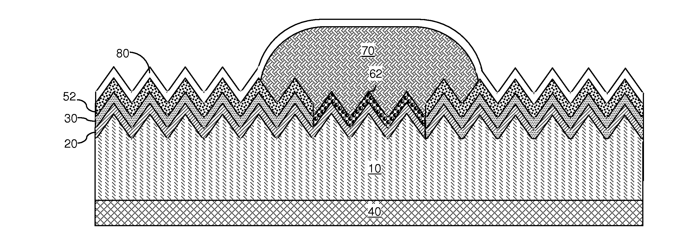
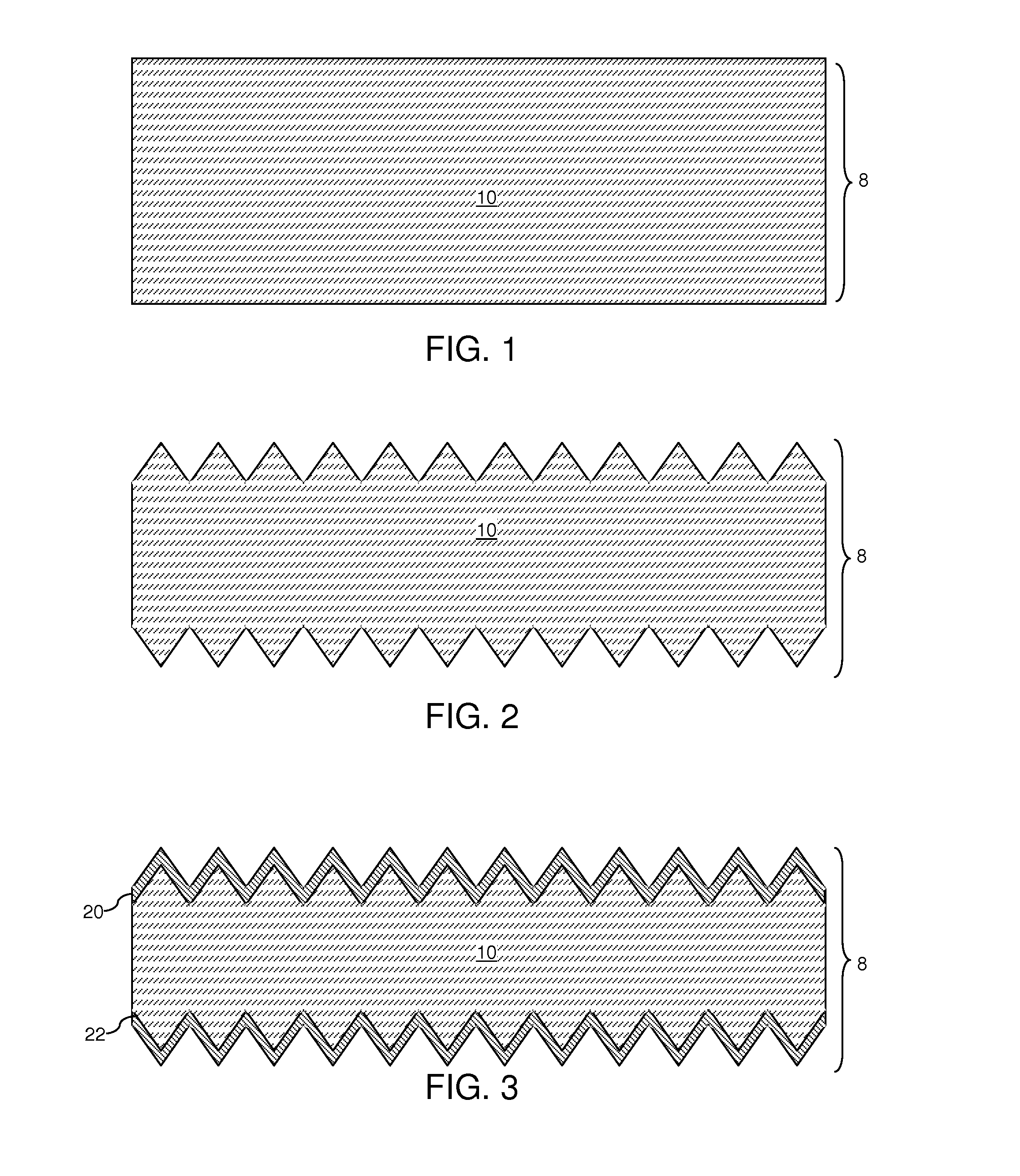
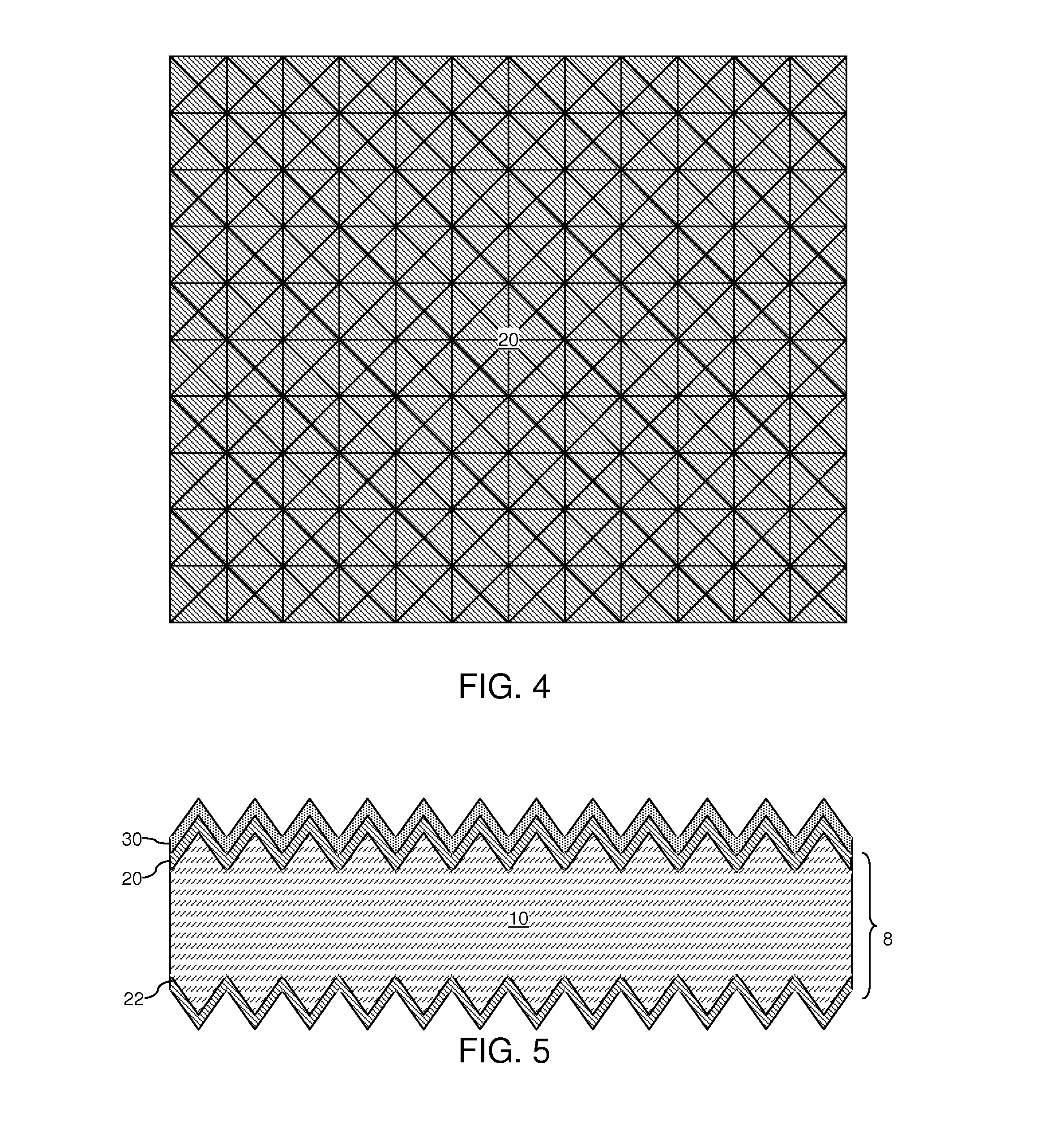
[0031]As stated above, the present disclosure relates to a method of forming an anti-reflective coating including a titania layer and a structure including the same, which are now described in detail with accompanying figures. It is noted that like reference numerals refer to like elements across different embodiments. The drawings are not necessarily drawn to scale.

[0032]Referring to FIG. 1, an exemplary structure according to an embodiment of the present disclosure includes a semiconductor substrate 8 that includes a semiconductor layer 10. The semiconductor layer 10 includes a semiconductor material. The semiconductor material can be silicon, germanium, a silicon germanium alloy, a silicon carbon alloy, a silicon germanium carbon alloy, a III-V compound semiconductor material, a II-VI compound semiconductor material, or any other semiconductor material known in the art. The semiconductor material of the semiconductor substrate can be single crystalline, polycrystalline, or amorph...


PUM

PropertyMeasurementUnit
temperatureaaaaaaaaaa
thicknessesaaaaaaaaaa

Abstract

A stack of a first anti-reflective coating (ARC) layer and a titanium layer is formed on a front surface of a semiconductor substrate including a p-n junction, and is subsequently patterned so that a semiconductor surface is physically exposed in metal contact regions of the front surface of the semiconductor substrate. The remaining portion of the titanium layer is converted into a titania layer by oxidation. A metal layer is plated on the metal contact regions, and a copper line is subsequently plated on the metal layer or a metal semiconductor alloy derived from the metal layer. A second ARC layer is deposited over the titania layer and the copper line, and is subsequently patterned to provide electrical contact to the copper line.

Description

BACKGROUND[0001]The present disclosure generally relates to an anti-reflective coating, and particularly to a method of forming an anti-reflective coating including a titania layer and a structure including the same. Further, the present disclosure relates to a method of forming an anti-reflective coating that has multiple layers including with a structure that includes dual anti-reflective coating layers.[0002]Light that impinges onto a front surface of a photovoltaic device passes through the front surface and generates an electron-hole pair within the semiconductor material. An electrostatic field generated by the p-n junction causes the electrons generated by the light to move toward the n-type material, and the holes generated by the light to move toward the p-type material. Contacts are made to the front side and the back side of the photovoltaic device to collect the charge carriers, thereby providing electromotive force for the photovoltaic device.[0003]Reflection of light a...

Claims


Application Information

Patent Timeline
Patent Type & Authority Applications(United States)
IPC IPC(8): H01L31/0216H01L31/18
CPCH01L31/02168H01L31/18H01L31/022425H01L31/02363H01L31/068H01L31/1804Y02E10/547Y02P70/50Y02E10/52
Inventor PAPA RAO, SATYAVOLU S.FISHER, KATHRYN C.HOVEL, HAROLD J.HUANG, QIANGHUANG, SUSANKIM, YOUNG-HEE
Owner GLOBALFOUNDRIES INC
Learn More