Method and system for CMOS image sensing device

Active Publication Date: 2011-08-04
SEMICON MFG INT (SHANGHAI) CORP +1
View PDF15 Cites 6 Cited by
  • Summary
  • Abstract
  • Description
  • Claims
  • Application Information

AI Technical Summary

Benefits of technology

[0011]This invention is directed to imaging techniques. More particularly, embodiments of the invention provide a method and system for capturing images on CMOS color sensors. Merely by way of exam

Problems solved by technology

With oil paintings, artists have been able to capture real world images with accuracy, but the fidelity of paintings is no match to photography.
While the increase resolution of image sensors often improve image resolution, the decreased pixel size and increase noise level

Method used


Image

  • Method and system for CMOS image sensing device
  • Method and system for CMOS image sensing device
  • Method and system for CMOS image sensing device

Examples


Embodiment Construction

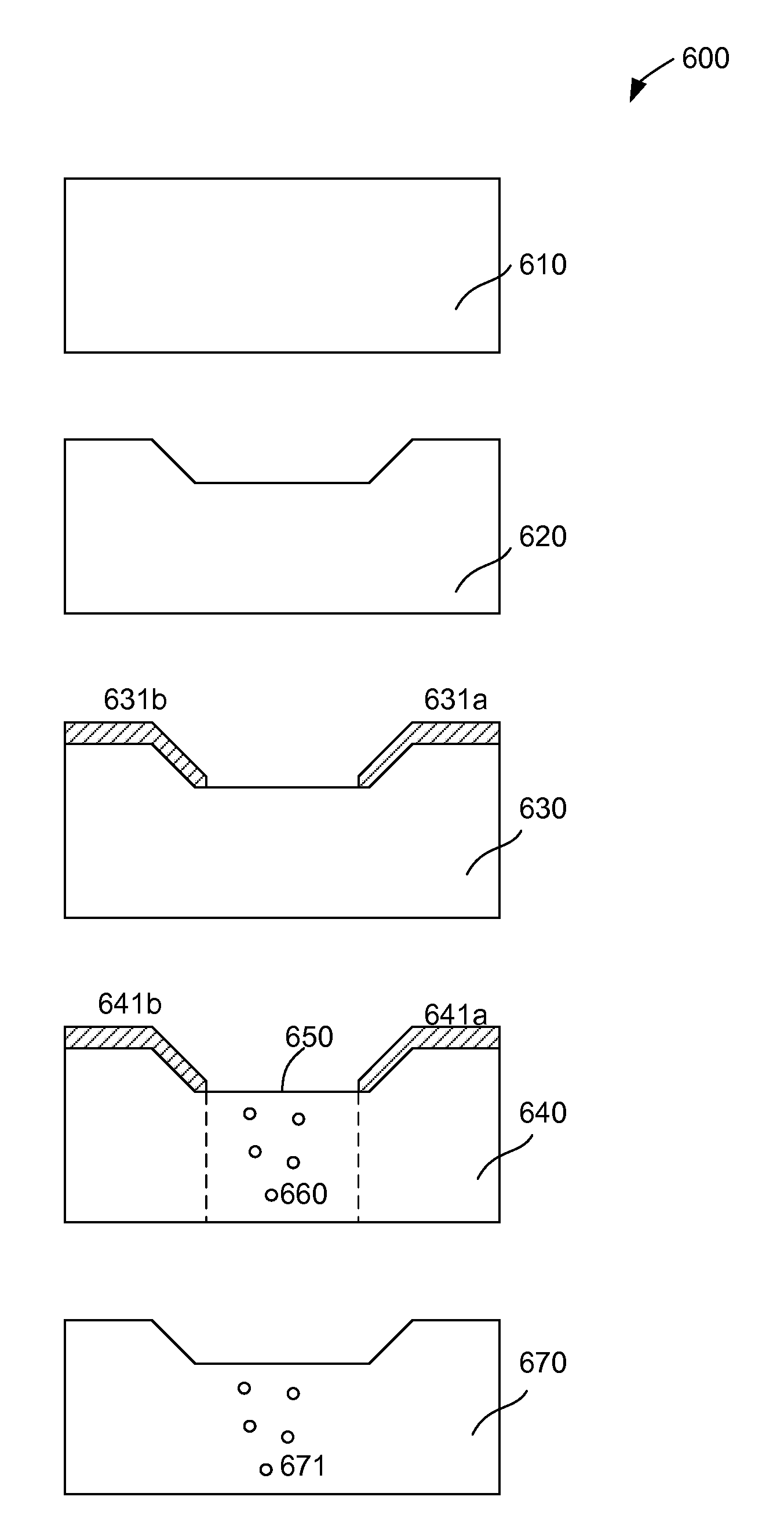
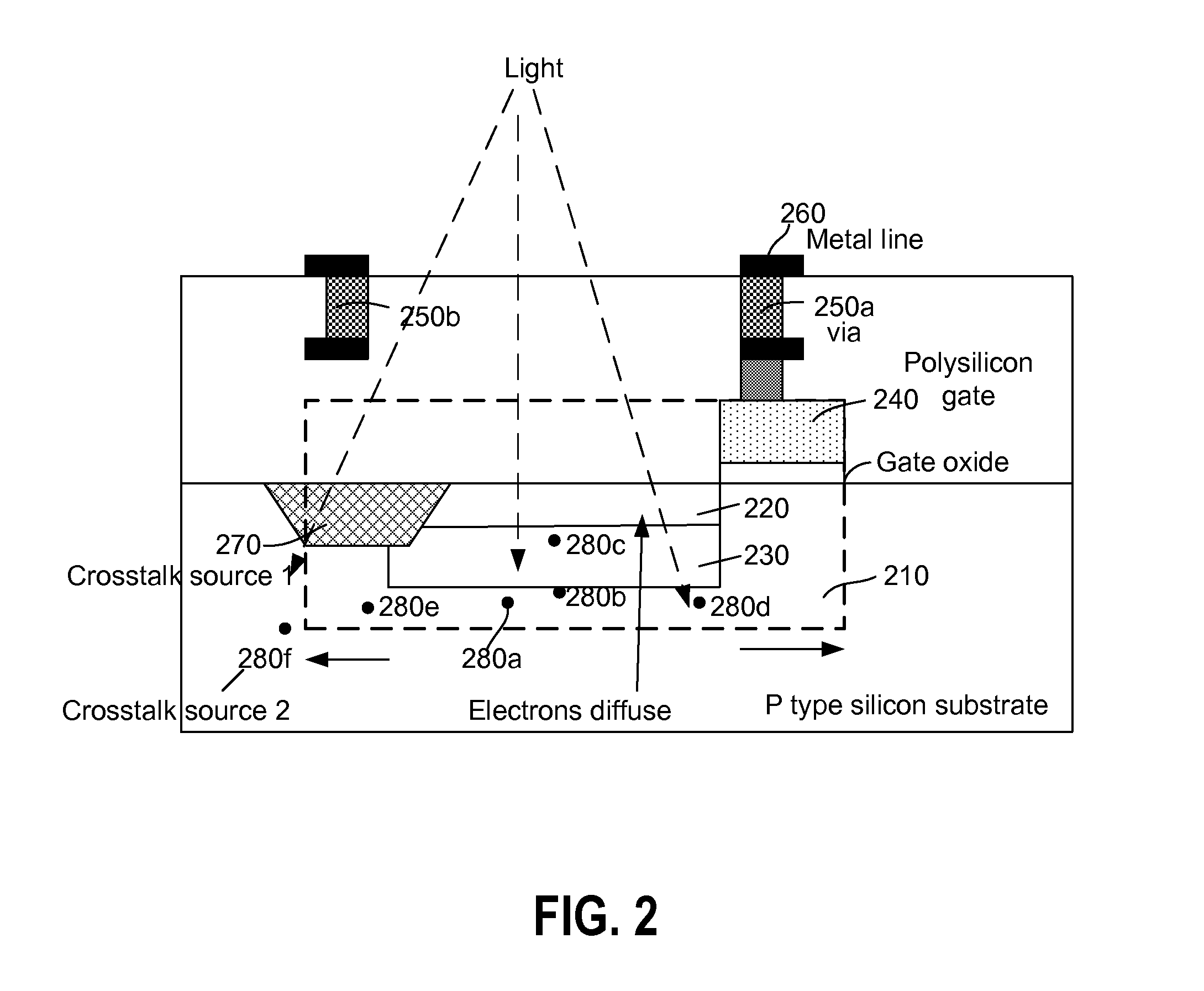
[0024]This invention is directed to imaging techniques. More particularly, embodiments of the invention provide a method and system for capturing images on CMOS color sensors. Merely by way of example, embodiments of the invention have been used to reduce and eliminate blooming effects in image capturing. But it would be recognized that the invention has a much broader range of applicability.

[0025]As discussed above, CMOS image sensors have various limitations. For example, the capability of image sensor is often measure by the number of image sensors (or pixels). In the recent years, camera makers have been racing one another for producing new cameras with higher pixel count. The resolution of CMOS image sensor has been increasing as pixel size shrink together with the MOS transistor channel length. While the increase resolution of image sensors often improve image resolution, the decreased pixel size and increase noise level have become obstacles for improved image quality. As a r...


PUM


Abstract

Method and system for manufacturing CMOS image sensing device with reduced blooming. The method includes a step for providing a substrate material. The substrate material can be characterized by a first dimension and a second dimension. In addition, the method includes a step for defining an active region on the substrate material. The active region is characterized by a third dimension and a fourth dimension. The method further includes a step for defining a non-active region on the substrate material. The non-active region is different from the active region. The non-active region is characterized by a fifth dimension and a sixth dimension, the non-active region including a silicon material. The method includes a step for defining a depletion region within the active region. In addition, the method includes a step for forming an n-type region positioned above the depletion region.

Description

CROSS-REFERENCES TO RELATED APPLICATIONS[0001]This application claims priority to Chinese Patent No. 200910104789.8 filed on Aug. 28, 2009, commonly assigned and hereby incorporated by reference for all purposes.BACKGROUND OF THE INVENTION[0002]This invention is directed to imaging techniques. More particularly, embodiments the invention provide a method and system for capturing images on CMOS color sensors. Merely by way of example, embodiments of the invention have been used to reduce and eliminate blooming effects in image capturing. But it would be recognized that the invention has a much broader range of applicability.[0003]To capture vivid imageries have long been an endeavor that persisted as long as the human race itself. As early as the Stone Age, people tried to capture of what they see with cave drawings. Over the thousands of years, artists developed techniques for capturing images with paint brushes and canvases. With oil paintings, artists have been able to capture rea...

Claims


Application Information

Patent Timeline
IPC IPC(8): H04N5/335H01L31/18H01L27/146
CPCH01L21/822H04N5/374H01L27/146Y02P70/50H04N25/76H04N23/54H01L27/14603H01L27/1463H01L27/14636H01L27/14643
Inventor ZHU, HONGYANG, JIANPING
Owner SEMICON MFG INT (SHANGHAI) CORP
Why Eureka
Try Eureka