Semiconductor device having silicon interposer on which semiconductor chip is mounted

a silicon interposer and semiconductor chip technology, applied in the direction of semiconductor devices, semiconductor/solid-state device details, electrical apparatus, etc., can solve the problems of unignorable level of signal quality degradation, long length of signal lines arranged on silicon interposers, and shortening the length of signal lines

Active Publication Date: 2014-01-02
LONGITUDE LICENSING LTD
View PDF3 Cites 37 Cited by
  • Summary
  • Abstract
  • Description
  • Claims
  • Application Information

AI Technical Summary

Problems solved by technology

However, in the silicon interposer described in Japanese Patent Application Laid-open Nos. 2007-12848 and 2009-110983, a current return path accompanied by transmission of signals is formed within a silicon substrate, and thus there is a problem that, when the frequency of a signal to be transmitted becomes high, the quality of the signal is degraded.
However, in a semiconductor device of a type in which a plurality of semiconductor chips are respectively mounted on different planes on a silicon interposer, the length of signal lines arranged on the silicon interposer becomes long, and the degradation of the signal quality becomes an unignorable level.
Furthermore, silicon interposers proposed in recent years have approximately 2000 sig...

Method used


Image

  • Semiconductor device having silicon interposer on which semiconductor chip is mounted
  • Semiconductor device having silicon interposer on which semiconductor chip is mounted
  • Semiconductor device having silicon interposer on which semiconductor chip is mounted

Examples


Embodiment Construction

[0022]Preferred embodiments of the present invention will be explained below in detail with reference to the accompanying drawings.

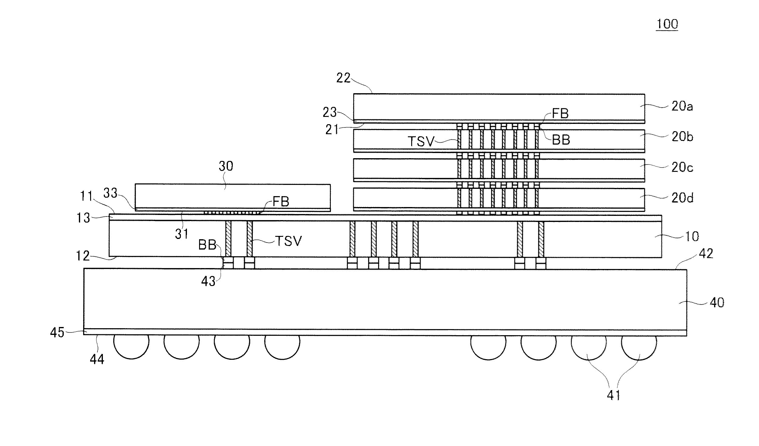
[0023]Referring now to FIG. 1, the semiconductor device 100 according to the first embodiment of the present invention includes an interposer 10, for example, a silicon interposer 10 mounted on a package substrate 40 and a plurality of memory chips 20a to 20d and a logic chip 30 mounted on the silicon interposer 10. Each of the silicon interposer 10, the memory chips 20a to 20d, and the logic chip 30 is a semiconductor chip integrated on a semiconductor substrate such as silicon. The memory chips 20a to 20d are memory devices such as a DRAM (Dynamic Random Access Memory), and the logic chip 30 is a control device that controls the memory chips 20a to 20d. Meanwhile, the package substrate 40 is a circuit substrate formed of resin and the like, and the package substrate 40 maintains the mechanical strength of the semiconductor device 100 and functions as a...


PUM


Abstract

Disclosed herein is a device that includes a silicon interposer having wiring lines on first and second wiring layers. The wiring lines includes first, second and third wiring lines provided on the first wiring layer and a fourth wiring line provided on the second wiring layer. The third wiring line is arranged between the first and second wiring lines on the first wiring layer. The fourth wiring line is overlapped with the third wiring line. Each of the first, second and fourth wiring lines conveys a power supply potential to first and second semiconductor chips mounted on the silicon interposer, and the third wiring line conveys a first signal communicated between the first and second semiconductor chips.

Description

BACKGROUND OF THE INVENTION[0001]1. Field of the Invention[0002]The present invention relates to a semiconductor device, and more particularly relates to a semiconductor device including a silicon interposer that is capable of transmitting a number of signals with a high signal quality.[0003]2. Description of Related Art[0004]In recent years, as a semiconductor device constituted by packaging a plurality of semiconductor chips, a semiconductor device using a silicon interposer has been attracting attention. Differently from conventional multichip packages, because the semiconductor device using a silicon interposer does not use bonding wires and the like for connection between semiconductor chips and the silicon interposer, this type of semiconductor device can realize higher density mounting and higher speed transmission of signals as compared to multichip packages (see Japanese Patent Application Laid-open Nos. 2007-12848 and 2009-110983).[0005]However, in the silicon interposer d...

Claims


Application Information

Patent Timeline
IPC IPC(8): H01L23/48
CPCH01L23/48H01L23/147H01L23/49816H01L23/49827H01L23/49833H01L23/49838H01L23/50H01L23/5286H01L24/13H01L24/14H01L24/16H01L25/0652H01L25/0657H01L25/18H01L2224/13025H01L2224/14181H01L2224/16145H01L2224/16225H01L2225/06517H01L2924/1431H01L2924/1434H01L2924/15311H01L2924/157H01L2225/06513H01L2225/06541H01L2225/06572H01L2225/06548H01L2224/0557H01L2924/00014H01L2224/05554H01L2224/0401H01L23/481H01L2224/05552
Inventor HIRAISHI, ATSUSHISUGANO, TOSHIOTAKAI, YASUHIRO
Owner LONGITUDE LICENSING LTD
Why Eureka
Try Eureka