Inertial Sensor

a sensor and sensor technology, applied in the field ofinertial sensors, can solve the problems of deterioration in sensor sensitivity, change in detection electrode due to sensor sensitivity, asymmetrical distortion of detection electrodes, etc., and achieve the effect of reducing the influence of asymmetrical distortion of mems elements and reducing the influence of mems element distortion

Active Publication Date: 2014-01-09
HITACHI ASTEMO LTD
View PDF5 Cites 31 Cited by
  • Summary
  • Abstract
  • Description
  • Claims
  • Application Information

AI Technical Summary

Benefits of technology

[0021]Among effects of the present invention, a representative effect is illustrated below. In the inertial sensor, it is possible to further reduce the influence of asymmetri

Problems solved by technology

Problems explained below occur because of the deformation.
However, when a process for applying high pressure such as the transfer mold process is applied to an inertial sensor that satisfies such demands, asymmetrical distortion occurs in the detection electrode.
This causes deterioration in sensor sensitivity.
Second, distortion due to high pressure is explained. In the transfer mold process, when the resin is filled, high pressure of about 5 to 20 MPa is applied to the MEMS element. In such a high-pressure process, a change in the detection electrode due to the distortion of the MEMS element is also large compared with the process in the past. Therefore, even

Method used


Image

  • Inertial Sensor
  • Inertial Sensor
  • Inertial Sensor

Examples


first embodiment

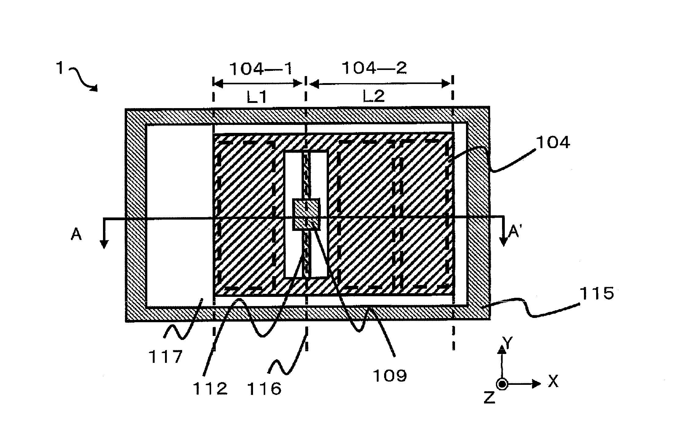
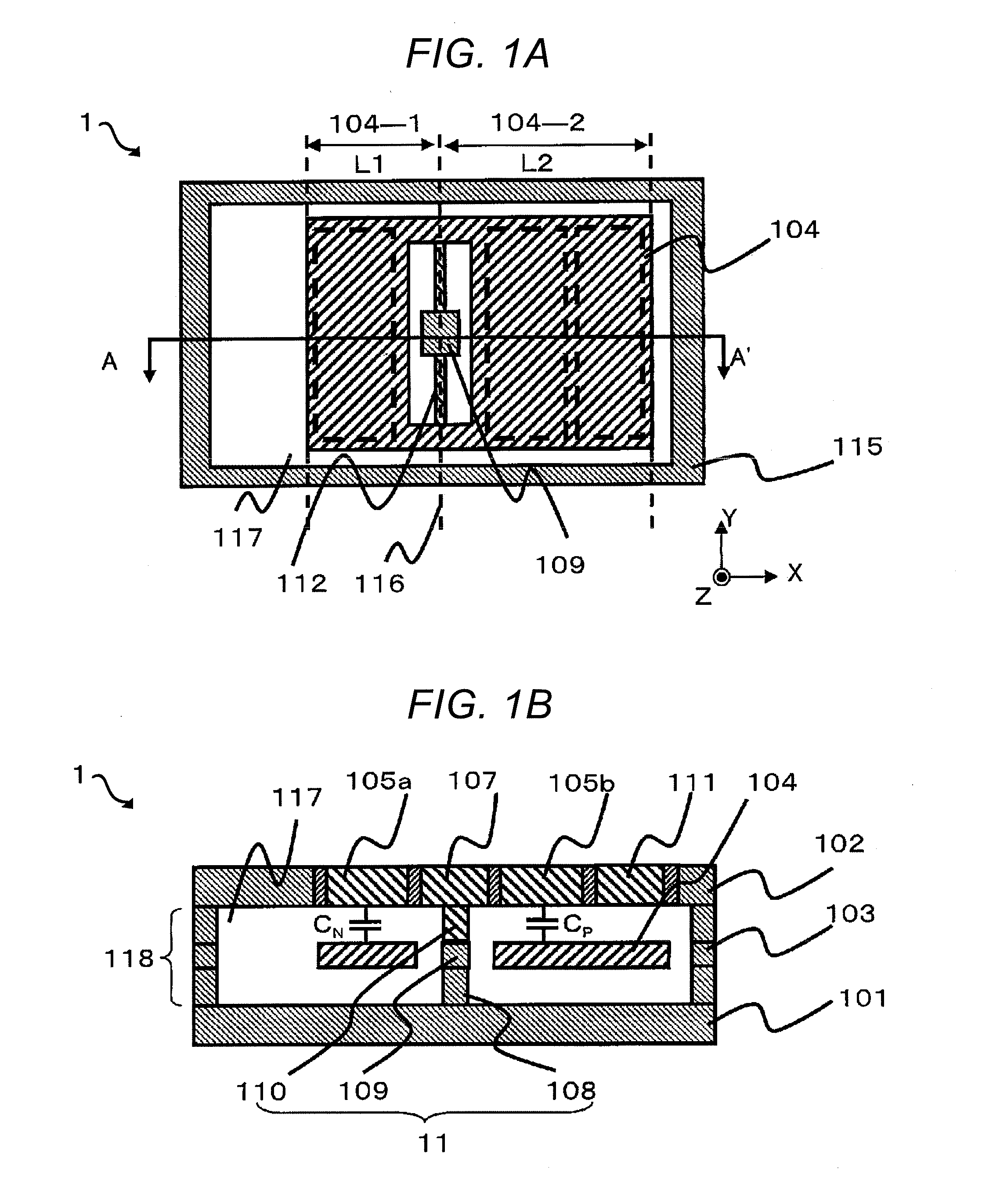
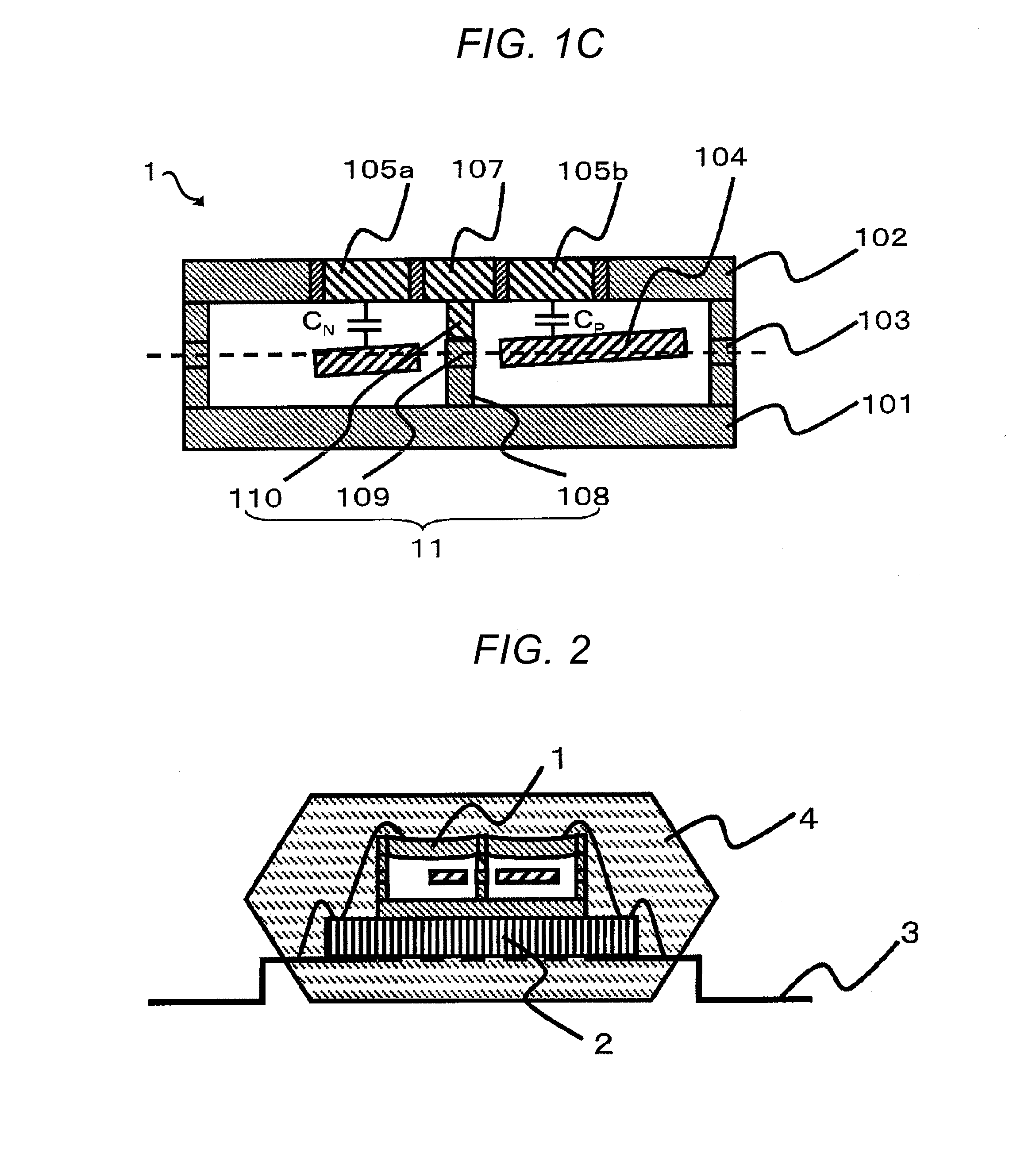
[0037]FIG. 1A is a sectional view of an MEMS element 1 in a first embodiment on the XY plane including a movable part 104. A portion of the movable part 104 opposed to detection electrodes 105a and 105b and a portion of the movable part 104 opposed to a diagnosis electrode 111 are indicated by dotted lines. FIG. 1B is a sectional view in an XZ plane of the MEMS element 1 shown in FIG. 1A taken along a line A-A′.

[0038]In the MEMS element 1 shown in FIGS. 1A and 1B, in a cavity 117 surrounded by a first silicon wafer substrate 101, a second silicon wafer substrate 102 provided above the first silicon wafer substrate 101, and a sidewall 118, the movable part 104 formed on a silicon wafer substrate 103, an elastic beam 112, a supporting section 109, and a frame body 115 are provided. In this way, an inertial sensor according to this embodiment is desirably formed by a three-layer structure including three silicon wafer substrates.

[0039]The supporting section 109 is provided in the cente...

second embodiment

[0056]A second embodiment is explained. Detailed explanation of components same as the components in the first embodiment is omitted. Differences from the first embodiment are mainly explained.

[0057]FIG. 3A is a sectional view in an XY plane of the MEMS element 1 according to this embodiment. A portion of a first movable part 204 opposed to detection electrodes 205a and 205b and a portion of a second movable part 206 opposed to diagnosis electrodes 211a and 211b are indicated by dotted lines. FIG. 3B is a sectional view in an XZ plane of FIG. 3A taken along a line A-A′.

[0058]In the MEMS element 1 according to this embodiment, in a cavity surrounded by a first silicon wafer substrate 201, a second silicon wafer substrate 202 provided above the first silicon wafer substrate 201, and a sidewall 218, the first movable part 204 and the second movable part 206 formed in a silicon wafer 203, elastic beams 212 and 213, a supporting section 209, and a frame body 215 are provided.

[0059]The su...

third embodiment

[0074]The configuration of an inertial sensor according to a third embodiment is explained with reference to FIGS. 5A and 5B.

[0075]FIG. 5A is a sectional view in an XY plane including a movable part 404 of the MEMS element 1 in this embodiment. Portions of the movable part 404 opposed to detection electrodes 405a and 405b and a diagnosis electrode 411 are indicated by dotted lines. FIG. 5B is a sectional view in an XZ plane of the MEMS element 1 shown in FIG. 5A taken along a line A-A′.

[0076]In the MEMS element 1 shown in FIGS. 5A and 5B, three silicon wafer substrates 401, 402, and 403 form a three-layer structure same as the three-layer structure in the first embodiment.

[0077]On the other hand, the third embodiment is different from the first embodiment in that the MEMS element 1 includes two supports 11 and 22. As in the first embodiment, the support 11 is a support including supporting sections 408a, 409a, and 410a that support the movable part 404. On the other hand, the suppor...


PUM


Abstract

A movable part rotates about a rotation axis, which passes through a support, when an inertial force in a detecting direction is applied to an inertial sensor. The movable part includes a first region and a second region displaced in a direction opposite to a direction of the first region when the inertial force is applied. A second substrate includes first and second detection electrodes opposed to the first and second regions, respectively. The first detection electrode and the second detection electrode are provided symmetrically with respect to the rotation axis. A cavity is provided symmetrically with respect to the rotation axis. In a direction perpendicular to the detecting direction and a direction in which the rotation axis extends, a length from the rotation axis to an end of the first region and a length from the rotation axis to an end of the second region are different.

Description

BACKGROUND OF THE INVENTION[0001]1. Field of the Invention[0002]The present invention relates to an inertial sensor.[0003]2. Background Art[0004]An inertial sensor manufactured by a machining technique of micro electro mechanical systems (MEMS) detects displacement of a movable part in order to measure an inertial force. The inertial sensor can measure an inertial force such as acceleration, an angular velocity, or angular acceleration by converting the displacement into an electric signal and processing the electric signal with an electronic circuit. In particular, a capacitance type inertial sensor detects the displacement as a change in the capacitance between a fixed detection electrode and a movable electrode. In the following explanation, a direction which is orthogonal to a principal plane of a substrate layer in which an elastic beam and a movable part are to be machined is referred to as an out-of-plane direction. For example, acceleration acting in the out-of-plane directi...

Claims


Application Information

Patent Timeline
IPC IPC(8): G01P15/125
CPCG01P15/125G01P15/0802G01P2015/0831
Inventor ZHANG, YUHUAJEONG, HEEWONYAMANAKA, KIYOKOHAYASHI, MASAHIDE
Owner HITACHI ASTEMO LTD
Why Eureka
Try Eureka