Image transfer process employing a hard mask layer

a technology of image transfer and mask layer, which is applied in the direction of instruments, transportation and packaging, printing, etc., can solve the problems of pattern transfer fidelity degradation, and achieve the effect of high-fidelity pattern transfer

Inactive Publication Date: 2014-01-23
IBM CORP
View PDF5 Cites 2 Cited by
  • Summary
  • Abstract
  • Description
  • Claims
  • Application Information

AI Technical Summary

Benefits of technology

[0004]At least one mask layer formed over a substrate includes at least one of a dielectric material and a metallic material. By forming a first pattern in one of the at least one mask layer, a patterned mask layer including said first pattern is formed. An overlying structure including a second pattern that includes at least one blocking area is formed over said patterned mask layer. Portion

Problems solved by technology

Thus, the fidelity of pattern transfer is degraded due to the lateral etching of the org

Method used


Image

  • Image transfer process employing a hard mask layer
  • Image transfer process employing a hard mask layer
  • Image transfer process employing a hard mask layer

Examples


first embodiment

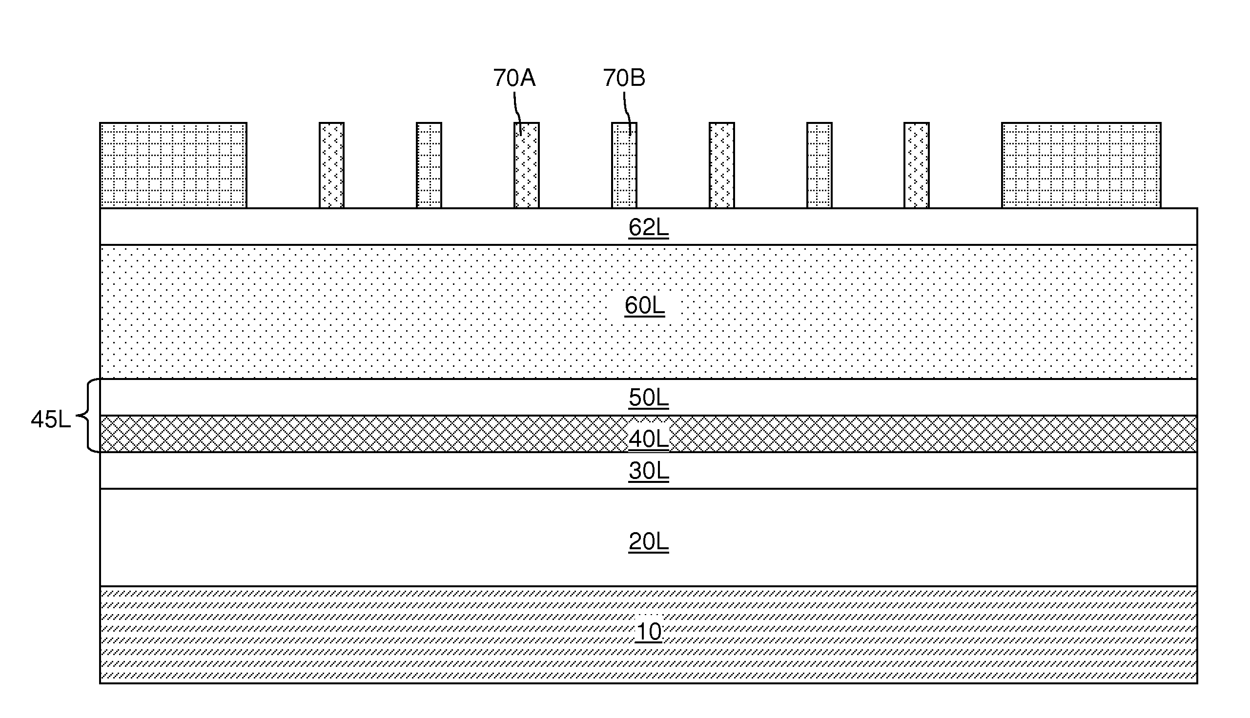
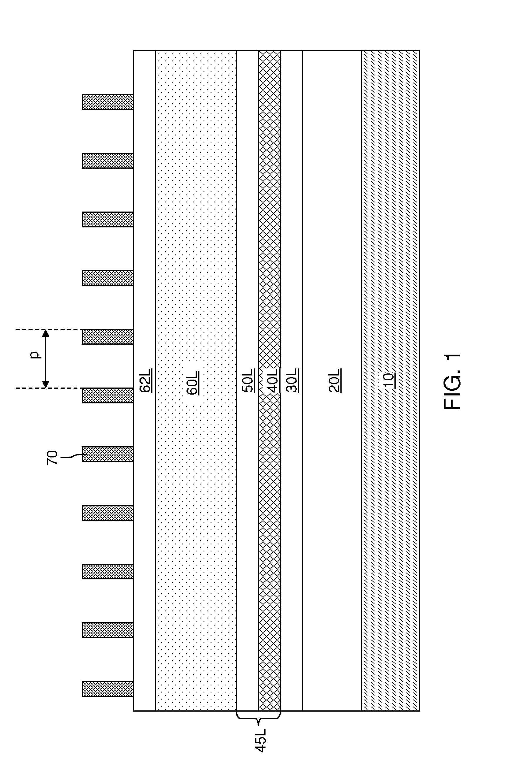
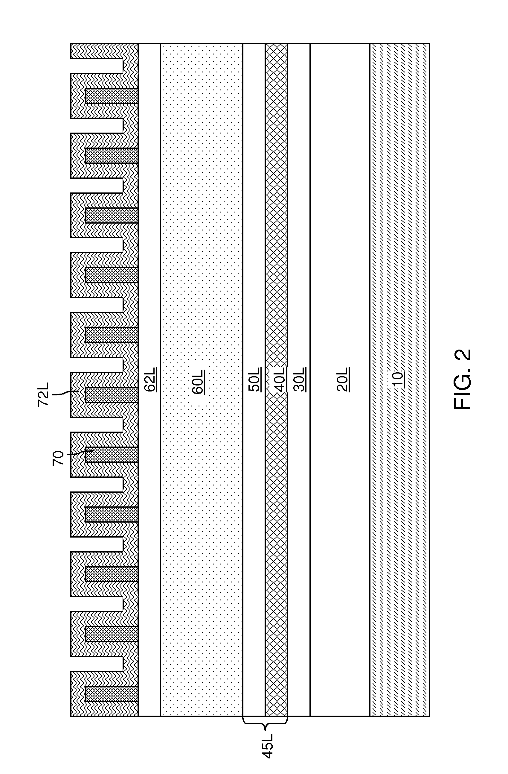
[0038]FIG. 1 is a vertical cross-sectional view of a first exemplary structure after deposition of an underlying material layer, and optional dielectric material layer, a dielectric mask layer, a metallic mask layer, a first organic planarizing layer (OPL), a first antireflective coating (ARC) layer, and mandrel structures according to the present disclosure.

[0039]Referring to FIG. 1, a first exemplary structure according to a first embodiment of the present disclosure includes a substrate 10 and a material stack formed thereupon. The substrate 10 can include a semiconductor substrate having semiconductor devices (not shown) therein. The semiconductor devices can include, for example, field effect transistors, junction transistors, diodes, resistors, capacitors, inductors, or any other semiconductor device known in the art. The substrate 10 may, or may not, include contact-level dielectric material layers (not shown) and / or interconnect level dielectric material layers (not shown) a...

fourth embodiment

[0126]Referring to FIG. 26, a fourth exemplary structure according to the present disclosure can be derived from the first exemplary structure of FIG. 1 by not forming the mandrel structures 70 and by applying and lithographically patterning a photoresist layer to form a patterned photoresist layer 80 including a first pattern. The patterned photoresist layer 80 can include a set of photoresist material portions.

[0127]The fourth exemplary structure illustrated in FIG. 26 is a lithographic structure, which includes the underlying material layer 20L located on the substrate 10; at least one mask layer 45L including at least one of a dielectric material and a metallic material and located over the underlying material layer 20L; the first organic planarizing layer (OPL) 60L located over the at least one mask layer 45L; the first antireflective coating (ARC) layer 62L located on the first OPL 60L; and the patterned structure of the patterned photoresist layer 80 located over the first AR...

fifth embodiment

[0129]Referring to FIG. 27, a fifth exemplary structure according to the present disclosure can be derived from the second exemplary structure of FIG. 18 by not forming the mandrel structures 70 and by applying and lithographically patterning a photoresist layer to form a patterned photoresist layer 80 including a first pattern. The patterned photoresist layer 80 can include a set of photoresist material portions.


PUM

PropertyMeasurementUnit
Thicknessaaaaaaaaaa
Dielectric polarization enthalpyaaaaaaaaaa
Structureaaaaaaaaaa

Abstract

At least one mask layer formed over a substrate includes at least one of a dielectric material and a metallic material. By forming a first pattern in one of the at least one mask layer, a patterned mask layer including said first pattern is formed. An overlying structure including a second pattern that includes at least one blocking area is formed over said patterned mask layer. Portions of said patterned mask layer that do not underlie said blocking area are removed. The remaining portions of the patterned mask layer include a composite pattern that is an intersection of the first pattern and the second pattern. The patterned mask layer includes a dielectric material or a metallic material, and thus, enables high fidelity pattern transfer into an underlying material layer.

Description

CROSS REFERENCE TO RELATED APPLICATION[0001]This application is a continuation of U.S. patent application Ser. No. 13 / 552,992, filed Jul. 19, 2012 the entire content and disclosure of which is incorporated herein by reference.BACKGROUND[0002]The present disclosure generally relates to a process for manufacturing semiconductor structures, and particularly to an image transfer process employing a hard mask layer to memorize a composite pattern, and structures for effecting the same.[0003]A trilayer lithography process as known in the art employs an organic material layer such as an amorphous carbon layer in order to transfer a composite image of two independent images. The sidewalls of the organic material layer are formed with a significant level of line edge roughness and line width roughness during a pattern transfer etch that forms a pattern in the organic material layer employing an overlying layer as a patterned mask because the organic material layer is prone to lateral etching...

Claims


Application Information

Patent Timeline
IPC IPC(8): B32B3/10
CPCH01L21/0337H01L21/0338H01L21/31144H01L21/32139Y10T428/24802
Inventor JUNG, RYAN O.KANAKASABAPATHY, SIVANANDA K.YIN, YUNPENG
Owner IBM CORP
Why Eureka
Try Eureka