Wiring substrate, multi-piece wiring substrate, and method for producing same

a wiring substrate and multi-piece technology, applied in the direction of printed circuit manufacturing, printed circuit aspects, conductive pattern formation, etc., can solve the problems of wiring substrate jumping out of the dent, failure to achieve the chucking of the wiring substrate, and failure to achieve the positioning of the wiring substrate in the dent, etc., to achieve accurate insertion, improve the productivity of ceramic wiring substrates, and accurate insertion

Inactive Publication Date: 2014-02-06
NGK SPARK PLUG CO LTD
View PDF0 Cites 2 Cited by
  • Summary
  • Abstract
  • Description
  • Claims
  • Application Information

AI Technical Summary

Benefits of technology

[0019]According to the wiring substrate of claim 1, since each of four side surfaces has a belt-like uneven surface including a plurality of alternate and parallel convex portions and concave portions which are formed so as to extend along the front surface and the back surface, even when relatively short claws of a chucking apparatus come into contact with the uneven surfaces of a pair of opposite side surfaces, chucking of the wiring substrate can be reliably achieved. In addition, since claws of a positioning jig are reliably hooked on the uneven surfaces, the wiring substrate can be accurately accommodated at a specific position in a dent of a product tray. Thus, the present invention can contribute to improvement of the productivity of ceramic wiring substrates.
[0020]According to the wiring substrate of claim 2, each of four side surfaces is in a form wherein an uneven surface is located on the side toward the front surface, and a fracture surface is located on the side toward the back surface; a form wherein a fracture surface is located on the side toward the front surface, and an uneven surface is located on the side toward the back surface; or a form wherein a pair of uneven surfaces are located on respective sides toward the front surface and the back surface, and a fracture surface is located between the paired uneven surfaces. Therefore, chucking of the wiring substrate can be reliably achieved by bringing a pair of relatively short claws of a chucking apparatus into contact with the uneven surfaces of a pair of opposite side surfaces. In addition, since claws of a positioning jig are reliably hooked on the uneven surfaces or the fracture surfaces, the wiring substrate can be accurately accommodated at a specific position in a dent of a product tray.
[0021]According to the wiring substrate of claim 3, each side surface has a fracture surface having a width which is 70% or more of the thickness of the wiring substrate, and an uneven surface adjacent to at least one of the front surface and the back surface and having a width which is 30% or less of the thickness of the wiring substrate. Therefore, there can be readily and reliably carried out sandwiching of the wiring substrate by bringing a pair of relatively short claws into contact with the uneven surfaces of the substrate (i.e., chucking of the wiring substrate), as well as accommodation of the wiring substrate by hooking claws of a positioning jig on the aforementioned uneven surfaces or relatively wide fracture surfaces.
[0022]According to the multi-piece wiring substrate array of claim 4, when the wiring substrate units of the product region are divided into individual pieces along the dividing grooves, there can be reliably produced a plurality of wiring substrates each having side surfaces having the aforementioned uneven surfaces.
[0023]According to the multi-piece wiring substrate array production method of claim 5, since a plurality of laser irradiation processes are carried out while gradually shifting the focal point of a laser beam so that the depth of the focal point, as measured from the front surface or back surface of a green sheet, in a laser irradiation process is greater than that in the preceding laser irradiation process, there can be produced a multi-piece wiring substrate array in which dividing grooves are reliably formed on at least one of the front surface and the back surface of a green sheet such that the aforementioned uneven surfaces provided on a pair of facing inner wall surfaces of each dividing groove are in line symmetry with each other.

Problems solved by technology

Therefore, when a chucking apparatus is employed for conveying each wiring substrate by means of a pair of opposing claws of the apparatus, since each claw tends to slip on a smooth groove surface of the corresponding side surface of the wiring substrate when the claw comes into contact with the groove surface, chucking of the wiring substrate may fail to be achieved.
Meanwhile, when individual wiring substrates are to be positioned in each of a plurality of dents of a product tray by means of a positioning jig after insertion of the wiring substrates in the dent, since the positioning jig may slip on a smooth groove surface of each side surface of a wiring substrate due to slight vibration, positioning of the wiring substrates in the dent may fail to be achieved.
In the worst case, there may arise a problem in that some wiring substrates jump out of the dent.

Method used


Image

  • Wiring substrate, multi-piece wiring substrate, and method for producing same
  • Wiring substrate, multi-piece wiring substrate, and method for producing same
  • Wiring substrate, multi-piece wiring substrate, and method for producing same

Examples


Embodiment Construction

[0037]Embodiments of the present invention will next be described.

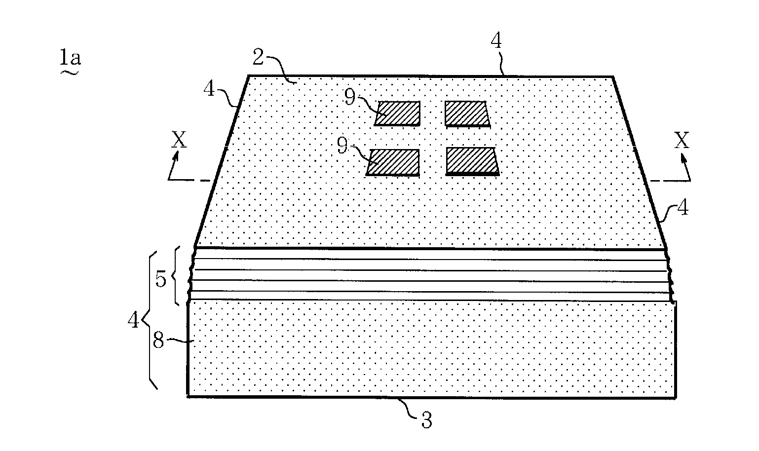
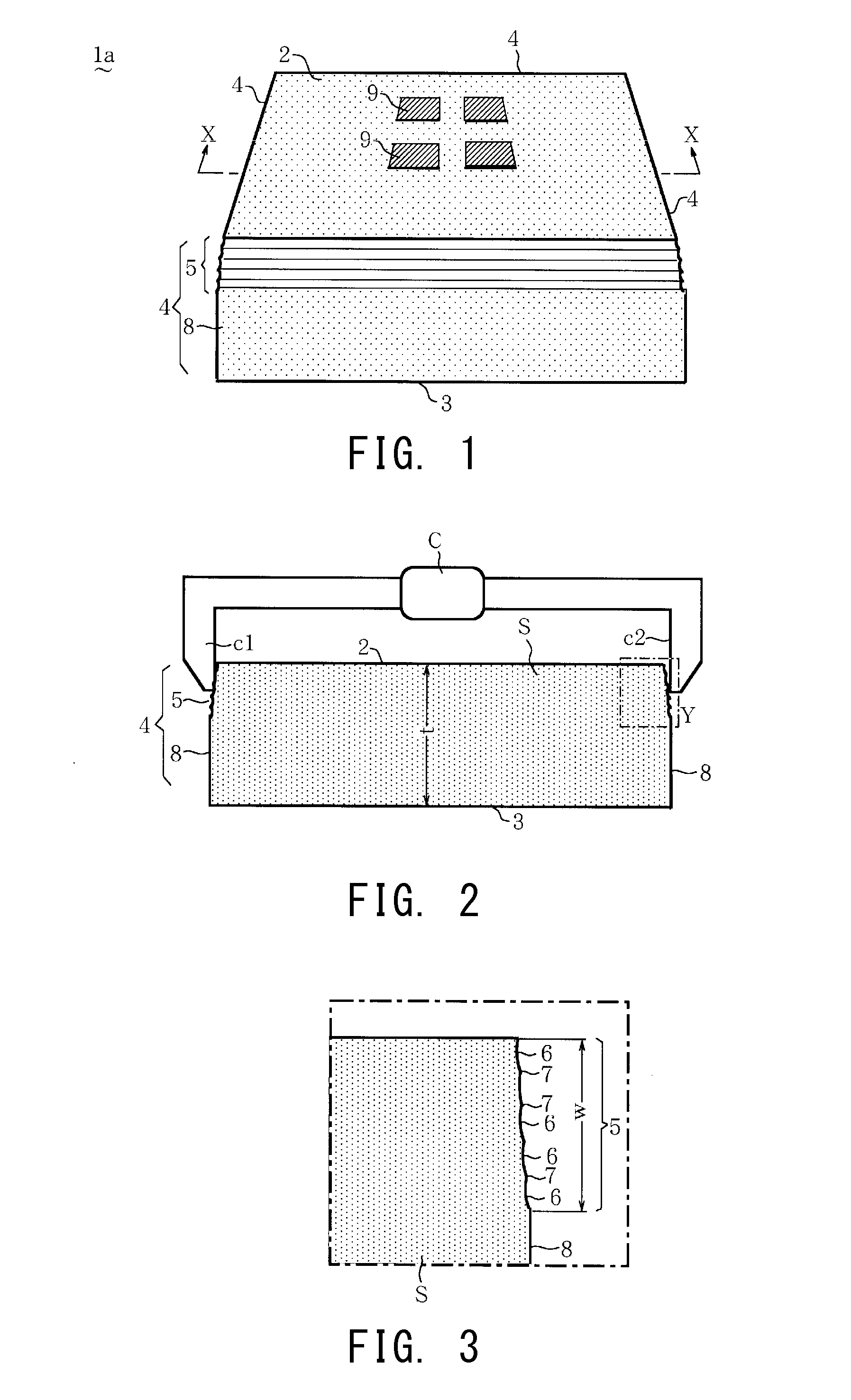
[0038]FIG. 1 is a perspective view of a wiring substrate 1a according to one embodiment of the present invention, as viewed from obliquely upward. FIG. 2 is a vertical cross-sectional view of the wiring substrate of FIG. 1 taken along line X-X. FIG. 3 is a partially enlarged view of a portion Y shown by dashed-dotted line in FIG. 2.

[0039]As shown in FIGS. 1 to 3, the wiring substrate 1a is formed of a ceramic laminate S, has a square (rectangular) shape in plan view, and has a front surface 2, a back surface 3, and four side surfaces 4 each being located between the front surface 2 and the back surface 3. Each side surface 4 has a belt-like uneven surface 5 including a plurality of alternate and parallel convex portions 7 and concave portions 6 which are formed so as to extend along the front surface 2, and also has a fracture surface 8 of the ceramic laminate S located between the uneven surface 5 and the back surfac...


PUM

PropertyMeasurementUnit
surface roughnessaaaaaaaaaa
frequencyaaaaaaaaaa
widthaaaaaaaaaa

Abstract

Provided are a ceramic wiring substrate having a side surface which realizes reliable chucking or hooking; a multi-piece wiring substrate array for providing a plurality of the wiring substrates; and a method for reliably producing the multi-piece wiring substrate array. The wiring substrate is formed of a ceramic material, has a square (rectangular) shape in plan view, and which has a front surface, a back surface, and side surfaces each being located between the front surface and the back surface, wherein each side surface has a belt-like uneven surface including a plurality of alternate and parallel convex portions and concave portions which are formed so as to extend along the front surface, and also has a fracture surface located on a side toward the back surface.

Description

TECHNICAL FIELD[0001]The present invention relates to a wiring substrate having a side surface which provides reliable chucking, etc. during conveyance thereof; to a multi-piece wiring substrate array for providing a plurality of the wiring substrates; and to a method for producing the multi-piece wiring substrate array.BACKGROUND ART[0002]Generally, ceramic wiring substrates are produced by dividing a multi-piece ceramic wiring substrate array into individual wiring substrates along dividing grooves provided on a front surface or a back surface of the wiring substrate array. In connection therewith, there has been proposed a method for producing a multi-piece wiring substrate array, in which a blade having a specific edge angle is pressed against a surface of a green sheet laminate at positions where dividing grooves are to be formed, so that breakage, burrs, etc. are less likely to occur at a metal layer located in a vicinity of the thus-formed dividing grooves during formation of...

Claims


Application Information

Patent Timeline
Patent Type & Authority Applications(United States)
IPC IPC(8): H05K1/02H05K3/10
CPCH05K3/0029H05K2203/1476H05K1/0306H05K2201/0909H05K3/0052H05K1/02H05K2201/09154H05K3/10Y10T29/49162H05K3/00
Inventor HASEGAWA, MASAMIHIRAYAMA, SATOSHIKITO, NAOKI
Owner NGK SPARK PLUG CO LTD
Why Eureka
Try Eureka