Ceramic multilayer substrate and method for manufacturing the same

a ceramic multi-layer substrate and ceramic technology, applied in the direction of printed circuit manufacturing, printed circuit aspects, electrical apparatus construction details, etc., can solve the problems of component mounting failure, impaired planarity (coplanarity) of ceramic multi-layer substrate, etc., to achieve excellent coplanarity, high properties, and efficient manufacturing

Active Publication Date: 2014-02-06
MURATA MFG CO LTD
View PDF7 Cites 0 Cited by
  • Summary
  • Abstract
  • Description
  • Claims
  • Application Information

AI Technical Summary

Benefits of technology

[0039]When the constraining layer is arranged between the internal conductors with about three or four of the ceramic layers disposed therebetween, the three or four ceramic layers between the constraining layer and the internal conductors shrink significantly in a thickness direction in a firing step. Therefore, the deformation of the ceramic layers due to the overlap of the internal conductors can be reliably absorbed.
[0040]In the case of forming a coil by arranging coil conductors in a ceramic multilayer substrate, the coil conductors (internal conductors), which preferably have the same shape, are arranged so as to overlap each other in the stacking direction and therefore a region of a substrate surface that corresponds to a region where the coil conductors are provided is likely to protrude to be convex. Applying a preferred embodiment of the present invention to such a ceramic multilayer substrate allows a ceramic multilayer substrate that is excellent in coplanarity to be obtained, which is particularly advantageous.
[0041]In the case of using a ceramic material containing a glass component to form the ceramic layers, a ceramic multilayer substrate having high properties can be efficiently manufactured through a firing step at a relatively low temperature of, for example, about 1,000° C. or lower, which is particularly advantageous.
[0042]The glass component diffuses from the ceramic layers into the constraining layer to increase the bonding strength between the constraining layer and the ceramic layers and the constraining layer prevents the ceramic layers from shrinking in a direction parallel or substantially parallel to a principal surface thereof. As a result, the shrinkage of the ceramic layers in a thickness direction thereof is promoted, the deformation (the increase in thickness) of the ceramic layers in a firing step is absorbed, and the coplanarity is significantly enhanced, which is advantageous.
[0043]A method for manufacturing a ceramic multilayer substrate according to another preferred embodiment of the present invention includes preparing a green laminate including a plurality of substrate ceramic green layers containing a substrate ceramic material powder; internal conductors being arranged on at least two of the substrate ceramic green layers, and at least a portion of one of the internal conductors arranged on one of the substrate ceramic green layer overlaps another internal conductor located on another substrate ceramic green layer in the stacking direction; and a constraining layer which is arranged on a layer different from layers on which the internal conductors are located, wherein the constraining layer overlaps, in the stacking direction, an internal conductor-overlapping region where at least two of the internal conductors overlapping each other in the stacking direction overlap each other, the constraining layer has a planar area not more than twice the planar area of the internal conductor-overlapping region, and the constraining layer contains an inorganic material powder that is not sintered at the sintering temperature of the substrate ceramic material powder and also includes firing the green laminate at a temperature at which the inorganic material powder is not sintered but the substrate ceramic material powder is sintered. Therefore, a ceramic multilayer substrate that has excellent substrate surface coplanarity can be efficiently manufactured.
[0044]In the case of forming the constraining layer by applying an inorganic material paste containing the inorganic material powder to one of the ceramic layers, the constraining layer can be readily formed so as to have an arbitrary shape. This allows a preferred embodiment of the present invention to be more effective.

Problems solved by technology

However, a region where internal conductors are arranged so as to overlap each other in a stacking direction has a more convex substrate surface as compared to a region where no internal conductors are provided and therefore the planarity (coplanarity) of a ceramic multilayer substrate is impaired.
This results in a problem that when electronic components (surface-mount components) are mounted on a surface of the ceramic multilayer substrate, the failure of component mounting occurs.

Method used


Image

  • Ceramic multilayer substrate and method for manufacturing the same
  • Ceramic multilayer substrate and method for manufacturing the same
  • Ceramic multilayer substrate and method for manufacturing the same

Examples


first preferred embodiment

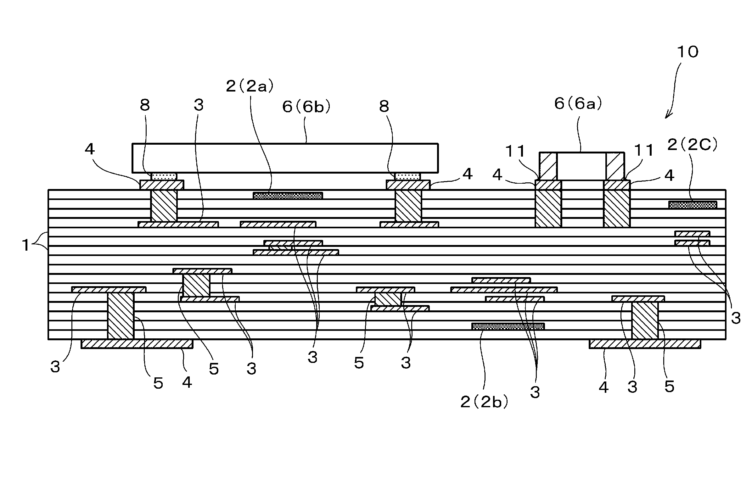
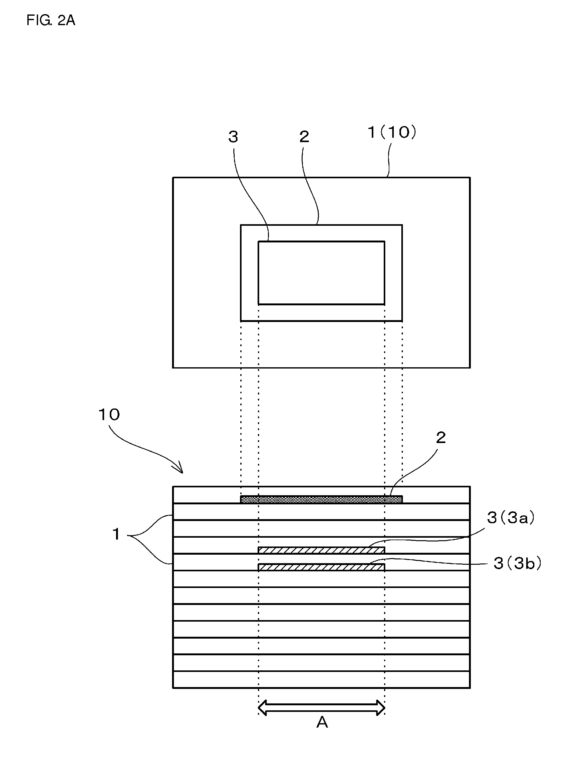
[0052]FIG. 1 is a schematic view illustrating the configuration of a ceramic multilayer substrate according to a first preferred embodiment of the present invention.

[0053]The ceramic multilayer substrate 10 includes ceramic layers 1 that are base layers, internal conductors 3 arranged between the layers, external conductors 4 located on surfaces of the substrate 10, and via-hole conductors 5 to achieve interlayer connection. The internal conductors 3 and external conductors 4 located on different layers are electrically connected to each other through the via-hole conductors 5.

[0054]Constraining layers 2 containing an inorganic material powder which is substantially unsintered are arranged on layers that are different from layers on which the internal conductors 3 are located so as to overlap, in a stacking direction, a region (an internal conductor-overlapping region) where at least two of the internal conductors 3 overlapping each other in the stacking direction overlap each other...

second preferred embodiment

[0111]FIG. 4 is a front sectional view illustrating the configuration of a ceramic multilayer substrate according to another preferred embodiment (a second preferred embodiment) of the present invention.

[0112]The ceramic multilayer substrate 10a includes ceramic layers 1 that are base layers, internal conductors 3 located between the layers, external conductors 4 located on surfaces, and via-hole conductors 5 for interlayer connection. The internal conductors 3 and external conductors 4 located on different layers are electrically connected to each other through the via-hole conductors 5.

[0113]The internal conductors 3 (3c) which are located in a thicknesswise central region of the ceramic multilayer substrate 10a and which overlap each other in a stacking direction are coil conductors that are connected to each other through via-hole conductors, which are not shown, to define a coil L.

[0114]In the ceramic multilayer substrate 10a, the ceramic layers 1 are preferably made of, for ex...


PUM

PropertyMeasurementUnit
temperatureaaaaaaaaaa
thicknessaaaaaaaaaa
thicknessaaaaaaaaaa

Abstract

A ceramic multilayer substrate includes stacked ceramic layers; internal conductors which are stacked with one of the ceramic layers therebetween, and are arranged such that at least a portion of the internal conductors overlap each other in a stacking direction; and a constraining layer which is arranged on a layer different from layers on which the internal conductors are located. The constraining layer overlaps, in the stacking direction, an internal conductor-overlapping region where at least two of the internal conductors overlapping each other in the stacking direction, has a planar area not more than twice the planar area of the internal conductor-overlapping region, and contains an unsintered inorganic material powder. The constraining layer has a planar area not more than one-half the planar area of the ceramic layers. The constraining layer is arranged so as to entirely cover the internal conductor-overlapping region.

Description

BACKGROUND OF THE INVENTION[0001]1. Field of the Invention[0002]The present invention relates to ceramic multilayer substrates and methods for manufacturing the same and particularly relates to a ceramic multilayer substrate having good surface planarity and excellent component mountability, and a method for manufacturing the same.[0003]2. Description of the Related Art[0004]In recent years, ceramic multilayer substrates having wiring conductors that are three-dimensionally arranged have been widely used for various applications.[0005]The following substrate has been proposed as one of the ceramic multilayer substrates: a ceramic multilayer substrate having a configuration in which via-hole conductors and internal conductors are provided in a laminate including a plurality of stacked ceramic layers, in which external conductors are located on surfaces thereof, and in which the internal conductors are connected to the external conductors through the via-hole conductors (see, for exam...

Claims


Application Information

Patent Timeline
Patent Type & Authority Applications(United States)
IPC IPC(8): H05K1/02H05K3/00
CPCH05K3/00H05K1/0298H05K3/4629H05K2201/0187H05K2201/09136H05K2201/09672
Inventor OTSUBO, YOSHIHITO
Owner MURATA MFG CO LTD
Why Eureka
Try Eureka