Inhibiting propagation of imperfections in semiconductor devices

a technology of semiconductor devices and imperfections, applied in semiconductor/solid-state device testing/measurement, semiconductor devices, semiconductor/solid-state device details, etc., can solve problems such as silicon imperfections, yield losses, and imperfections on the surface of silicon that do not extend into functional circuits

Inactive Publication Date: 2014-02-13
GLOBALFOUNDRIES INC
View PDF3 Cites 8 Cited by
  • Summary
  • Abstract
  • Description
  • Claims
  • Application Information

AI Technical Summary

Benefits of technology

[0004]Aspects of the disclosure provide a method of inhibiting crack propagation in a silicon wafer. In one embodiment, a method of repairing an imperfection on a surface of a semiconductor device is disclosed. The method includes: screening for imperfections on a surface of a silicon wafer of a semiconductor device; and in response to at least one imperfection on the surface of the silicon wafer, depositing a material on the surface of the silicon wafer.

Problems solved by technology

During module final tests, yield losses can be due to silicon imperfections (i.e., cracks, dings, nicks, pits, scratches, etc.) on the backside of the wafer or die.
However, some imperfections on the surface of the silicon do not extend into the functional circuitry.
However, in flip chip technologies, or other technologies where the entire thickness of the silicon wafer is desired, BSG is not a viable method to remove the surface imperfections of the silicon wafer.

Method used


Image

  • Inhibiting propagation of imperfections in semiconductor devices
  • Inhibiting propagation of imperfections in semiconductor devices
  • Inhibiting propagation of imperfections in semiconductor devices

Examples


Embodiment Construction

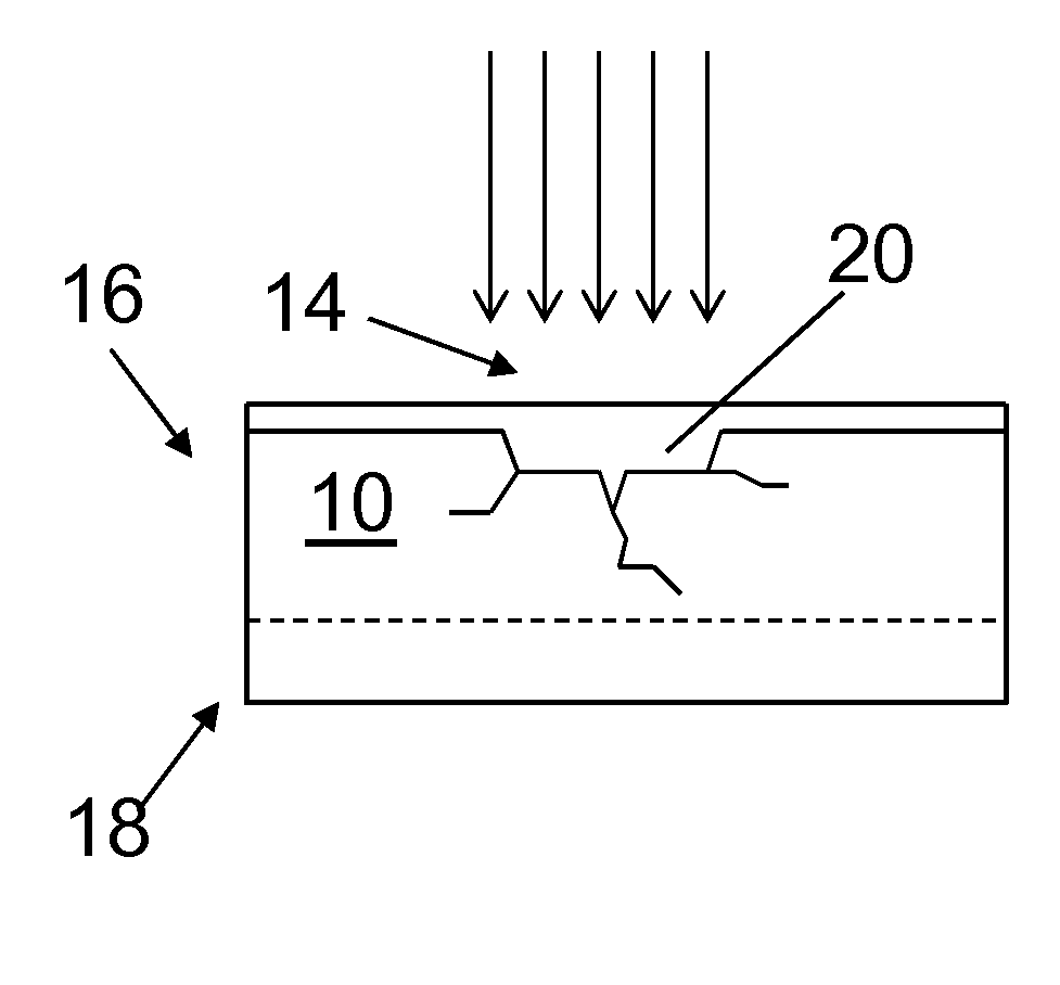
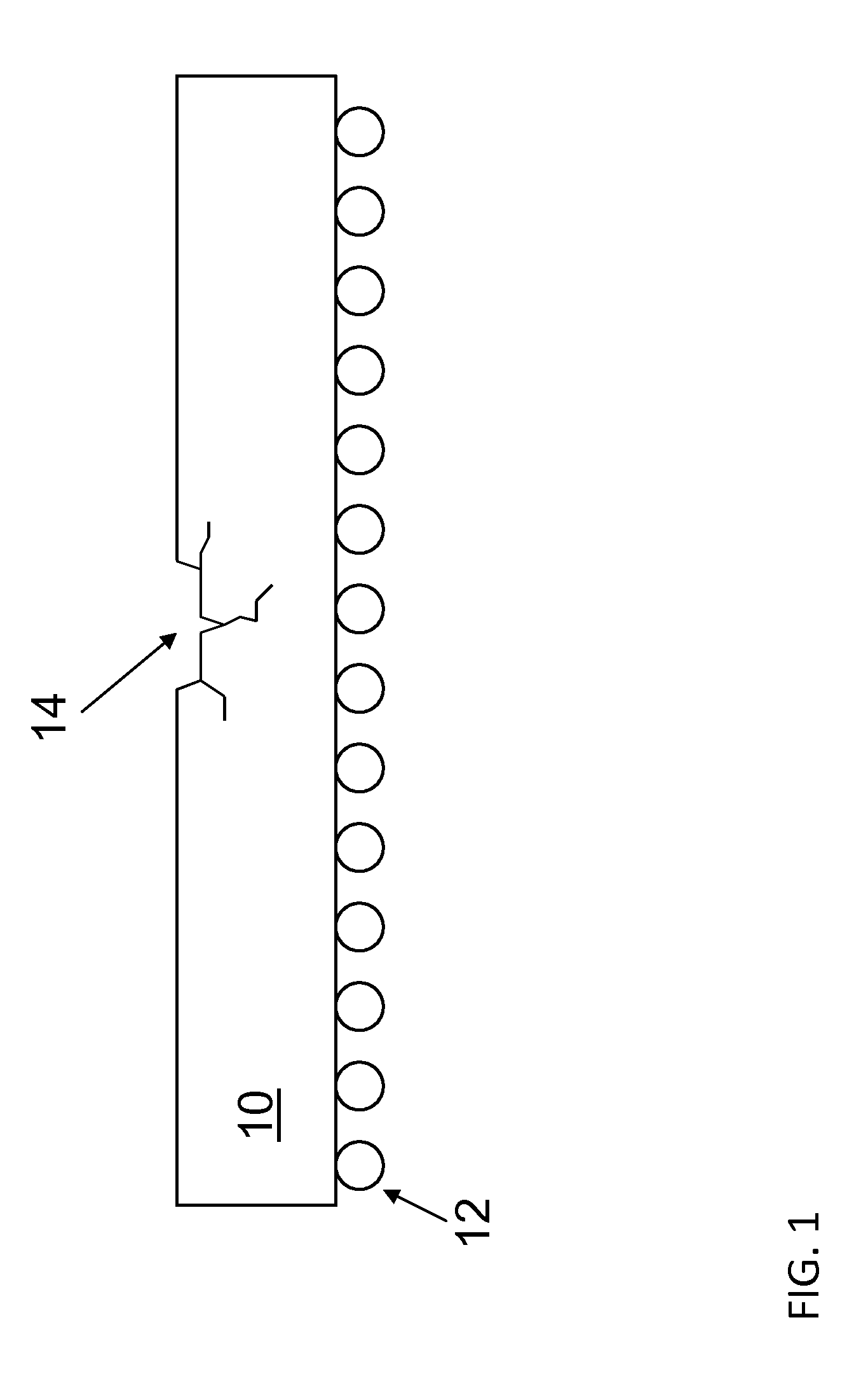
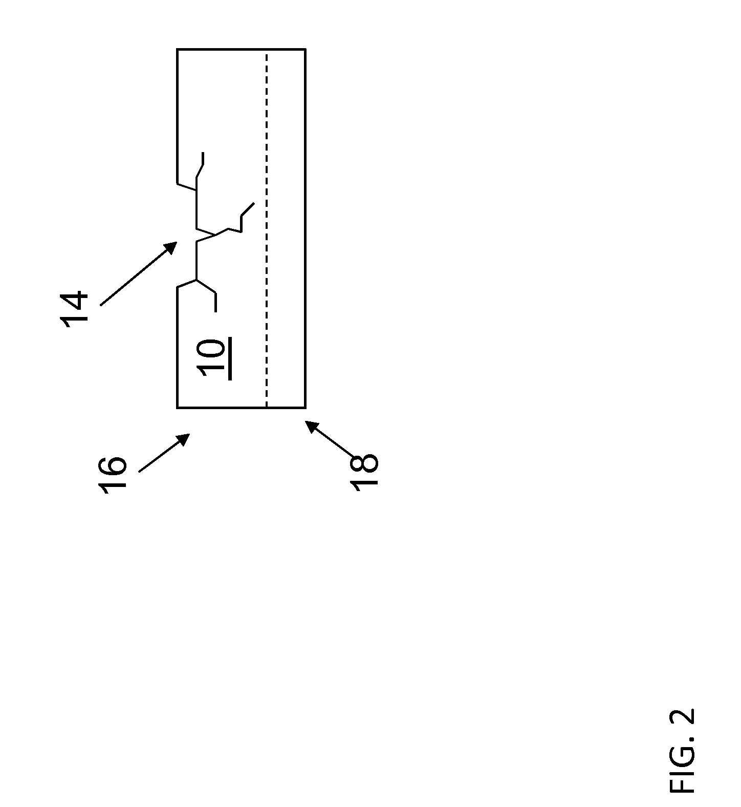
[0015]As mentioned above, this disclosure relates generally to semiconductor devices, and more particularly, to a method of repairing imperfections in silicon wafers to inhibit propagation of the imperfection.

[0016]During module final tests, yield losses can be due to silicon imperfections (i.e., cracks, dings, nicks, pits, scratches, etc.) on the backside of the wafer or die. These silicon imperfections start at the surface of the backside, but also extend further into the silicon and into the functional circuitry. However, some imperfections on the surface of the silicon do not extend into the functional circuitry. These imperfections are a concern because, although these imperfections are only at the surface (i.e., the inactive region) during the module final testing stage, temperature cycling during operation can propagate the imperfections into the functional circuitry (i.e., the active region).

[0017]To remove surface imperfections in the inactive region of the silicon wafers, ...


PUM

PropertyMeasurementUnit
acoustic microscopyaaaaaaaaaa
electrical testaaaaaaaaaa
organicaaaaaaaaaa

Abstract

Aspects of the disclosure provide a method of inhibiting crack propagation in a silicon wafer. In one embodiment, a method of repairing an imperfection on a surface of a semiconductor device is disclosed. The method includes: screening for imperfections on a surface of a silicon wafer of a semiconductor device; and in response to at least one imperfection on the surface of the silicon wafer, depositing a material on the surface of the silicon wafer.

Description

FIELD OF THE INVENTION[0001]The disclosure relates generally to semiconductor devices, and more particularly, to a method of repairing imperfections in silicon wafers to inhibit propagation of the imperfections.BACKGROUND[0002]During module final tests, yield losses can be due to silicon imperfections (i.e., cracks, dings, nicks, pits, scratches, etc.) on the backside of the wafer or die. These silicon imperfections start at the surface of the backside, but also extend further into the silicon and into the functional circuitry. However, some imperfections on the surface of the silicon do not extend into the functional circuitry. These imperfections are a concern because, although these imperfections are only at the surface during the module final testing stage, temperature cycling during operation can propagate the imperfections into the functional circuitry.[0003]Backside grinding (BSG) is a method to remove these surface imperfections by grinding down the thickness of the silicon ...

Claims


Application Information

Patent Timeline
Patent Type & Authority Applications(United States)
IPC IPC(8): H01L21/312H01L29/34
CPCH01L22/12H01L22/20H01L2224/13H01L2924/10158H01L21/302H01L21/312H01L23/3171H01L21/31058H01L23/3178H01L29/34H01L29/32
Inventor AYOTTE, STEPHEN P.HILL, DAVID J.RICHARD, GLEN E.SULLIVAN, TIMOTHY M.TRUAX, HEATHER M.
Owner GLOBALFOUNDRIES INC
Why Eureka
Try Eureka