Light emitting device, electronic apparatus, and method of driving light emitting device

a technology of light emitting devices and electronic devices, which is applied in the direction of instruments, static indicating devices, etc., can solve the problems of difficult to achieve high precision of images, and achieve the effect of high precision

Inactive Publication Date: 2014-02-13
SEIKO EPSON CORP
View PDF2 Cites 8 Cited by
  • Summary
  • Abstract
  • Description
  • Claims
  • Application Information

AI Technical Summary

Benefits of technology

[0010]An advantage of some aspects of the invention is to provide a double-sided light emitting-type light emitting device capable of achieving high precision.
[0012]In the aspect of the invention, the first circuit for generating an image displayed on one side of the substrate and the second circuit for generating an image displayed on the other side of the substrate share one data line, and thus it is possible to reduce an area per one pixel as compared with the aspect (two data lines are provided for each pixel) of separately providing the data line corresponding to the first circuit and the data line corresponding to the second circuit. Accordingly, there is an advantage of achieving high precision of the image.
[0013]The light emitting device according to the aspect of the invention further includes a driving circuit that drives the pixel circuit, in a first period, the driving circuit sets the first switching element to be turned on and the second switching element to be turned off, and outputs the first data potential corresponding to a designation gradation of the first light emitting element to the data line, and in a second period after the first period, the driving circuit sets the first switching element to be turned off and the second switching element to be turned on, and outputs the second data potential corresponding to a designation gradation of the second light emitting element to the data line. In the aspect, in the first period, the first data potential output to the data line is supplied to the gate of the first driving transistor through the first switching element that is turned on. Accordingly, the driving current corresponding to the first data potential flows in the first light emitting element, and the first light emitting element emits light in a brightness corresponding to the driving current. In the second period, the second data potential output to the data line is supplied to the gate of the second driving transistor through the second switching element that is turned on. Accordingly, the driving current corresponding to the second data potential flows in the second light emitting element, and the second light emitting element emits light in a brightness corresponding to the driving current. That is, according to the aspect, it is possible to accurately perform display of one side and display of the other side of the substrate, and it is possible to provide a light emitting device capable of achieving high precision.
[0015]In the aspect, in the driving circuit, the selection direction of the first scanning line and the selection direction of the second scanning line are in the reverse direction to each other, and thus it is possible to arrange a state of viewing the image displayed on one side of the substrate from one side and a state of viewing the image displayed on the other side of the substrate from the other side. That is, according to the aspect, it is possible to prevent the image displayed on one side of the substrate and the image displayed on the other side from being inversed.

Problems solved by technology

Accordingly, there is a problem that it is difficult to achieve high precision of an image.

Method used


Image

  • Light emitting device, electronic apparatus, and method of driving light emitting device
  • Light emitting device, electronic apparatus, and method of driving light emitting device
  • Light emitting device, electronic apparatus, and method of driving light emitting device

Examples


first embodiment

A: First Embodiment

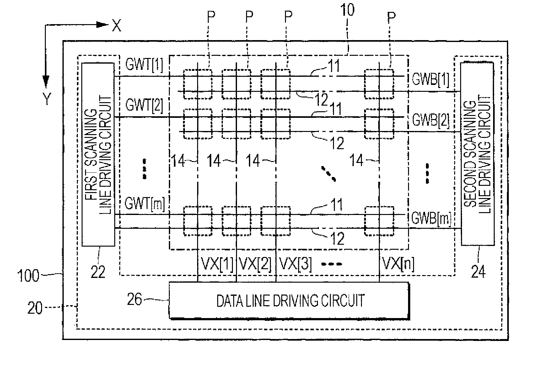
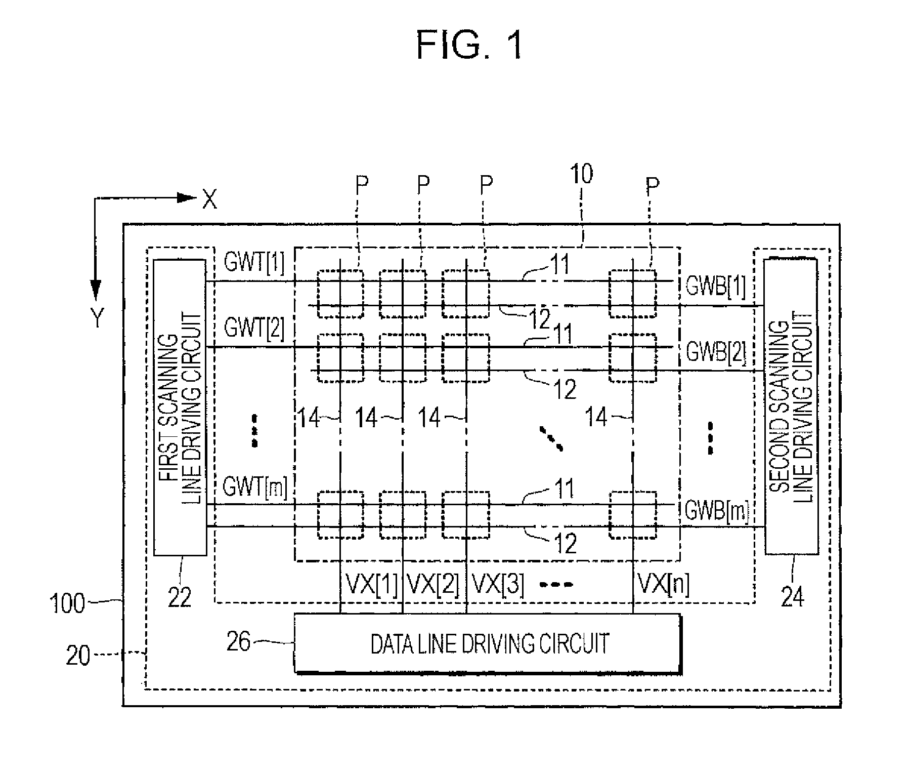
[0036]FIG. 1 is a block diagram illustrating a light emitting device 100 according to a first embodiment of the invention. The light emitting device 100 is mounted on an electronic apparatus as a display device displaying an image. As shown in FIG. 1, the light emitting device 100 includes an element unit 10 in which a plurality of pixel circuits P are arranged, and a driving circuit 20 driving the pixel circuits P. The driving circuit 20 includes a first scanning line driving circuit 22, a second scanning line driving circuit 24, and a data line driving circuit 26. The driving circuit 20 is mounted to be dispersed in, for example, a plurality of integrated circuits. At least a part of the driving circuit 20 may be configured by a thin-film transistor formed on a substrate with the pixel circuits P.

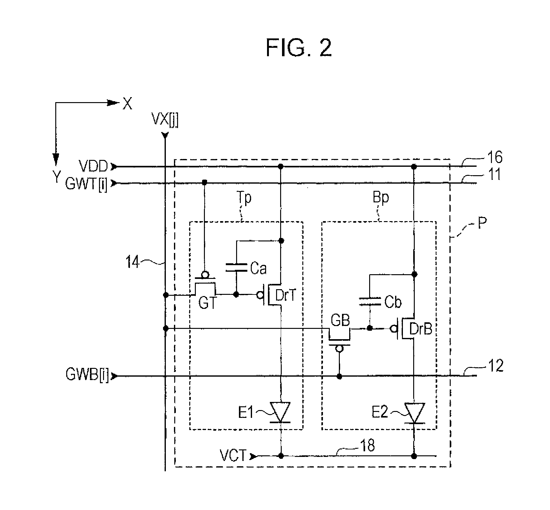
[0037]The element unit 10 is provided with m first scanning lines 11 extending in an X direction, m second scanning lines 12 corresponding to the first scanning lines 1...

second embodiment

B: Second Embodiment

[0063]A second embodiment is different from the first embodiment in that images to be displayed on the first substrate 31 side (hereinafter, referred to as “the front side of the panel”) and the second substrate 32 side (hereinafter, referred to as “the back side of the panel”) are the same, the driving circuit 20 sequentially selects the first scanning lines 11 in each horizontal scanning period H and sequentially selects the second scanning lines 12 in a reverse direction to the selection direction of the first scanning lines 11, and the data potential corresponding to the image data is output to the data lines 14. Hereinafter, specification thereof will be described.

[0064]FIG. 7 is a timing chart for describing a specific operation of a light emitting device according to the second embodiment. As shown in FIG. 7, the first scanning line driving circuit 22 sequentially sets the first scanning signals GWT [1] to GWT [m] to the active level (low level) for each o...

example 1

(1) Modified Example 1

[0071]The conductive types of various transistors included in the pixel circuits P are arbitrary. In the embodiments, all the various transistors included in the pixel circuits P are formed of the p-channel transistors, but are not limited thereto, for example, all the various transistors included in the pixel circuits P may be the N-channel type. For example, a part of the transistors among various transistors included in the pixel circuits P may be formed of the P-channel type, and the other transistors may be formed of the N-channel type.


PUM


Abstract

A light emitting device includes a pixel circuit and a data line provided between a first substrate and a second substrate opposed to each other. The pixel circuit includes a first circuit and a second circuit, the first circuit includes a first light emitting element and a first driving transistor connected in series to each other, and a first switching element provided between a gate of the first transistor and the data line, and outgoing light of the first light emitting element is output from the first substrate side. The second circuit includes a second light emitting element and a second driving transistor connected in series to each other, and a first switching element provided between a gate of the second driving transistor and the data line, and outgoing light of the second light emitting element is output from the second substrate side.

Description

REFERENCE TO COPENDING APPLICATIONS[0001]This application is a Divisional of application Ser. No. 13 / 038,669 filed Mar. 2, 2011, which claims priority from Japanese Patent Application JP 2010-054098 filed Mar. 11, 2010. The disclosure of the prior applications is hereby incorporated by reference herein in their entirety.BACKGROUND[0002]1. Technical Field[0003]The present invention relates to a light emitting device, an electronic apparatus, and a method of driving the light emitting device.[0004]2. Related Art[0005]Recently, various light emitting devices employing a light emitting element such as an organic light emitting diode (hereinafter, referred to as “OLED”) element called an organic EL (Electro Luminescent) element, a light emitting polymer element, or the like have been proposed. For example, in JP-A-2006-128077, a double-sided light emitting-type light emitting device capable of simultaneously displaying different images on one face and the other face of a panel is disclos...

Claims


Application Information

Patent Timeline
Patent Type & Authority Applications(United States)
IPC IPC(8): G09G3/32
CPCG09G3/3266H10K59/128G09G3/3275H10K59/131H10K2102/3031
Inventor OTA, HITOSHI
Owner SEIKO EPSON CORP
Why Eureka
Try Eureka