Method and system for providing dual magnetic tunneling junctions using spin-orbit interaction-based switching and memories utilizing the dual magnetic tunneling junctions

a magnetic tunneling junction and spin-orbit interaction technology, applied in the direction of inductance/transformer/magnet manufacture, magnetic bodies, instruments, etc., can solve the problem that memory employing the conventional mtj b>10/b> may have unacceptably high wer and may not be cured by an increase in voltag

Active Publication Date: 2014-02-27
SAMSUNG ELECTRONICS CO LTD
View PDF11 Cites 81 Cited by
  • Summary
  • Abstract
  • Description
  • Claims
  • Application Information

AI Technical Summary

Benefits of technology

[0012]FIG. 1 depicts a conventional magnetic junction.
[0013]FIG. 2 depicts write error rate versus voltage for a conventional spin transfer torque RAM.

Problems solved by technology

However, this also means that spin transfer based switching may require a larger write current.
In addition, it has been determined that the WER may be challenging to improve for shorter write current pulses.
Consequently, memories employing the conventional MTJ 10 may have unacceptably high WER that may not be cured by an increase in voltage.
Such a reduction in signal is undesirable.

Method used


Image

  • Method and system for providing dual magnetic tunneling junctions using spin-orbit interaction-based switching and memories utilizing the dual magnetic tunneling junctions
  • Method and system for providing dual magnetic tunneling junctions using spin-orbit interaction-based switching and memories utilizing the dual magnetic tunneling junctions
  • Method and system for providing dual magnetic tunneling junctions using spin-orbit interaction-based switching and memories utilizing the dual magnetic tunneling junctions

Examples


Embodiment Construction

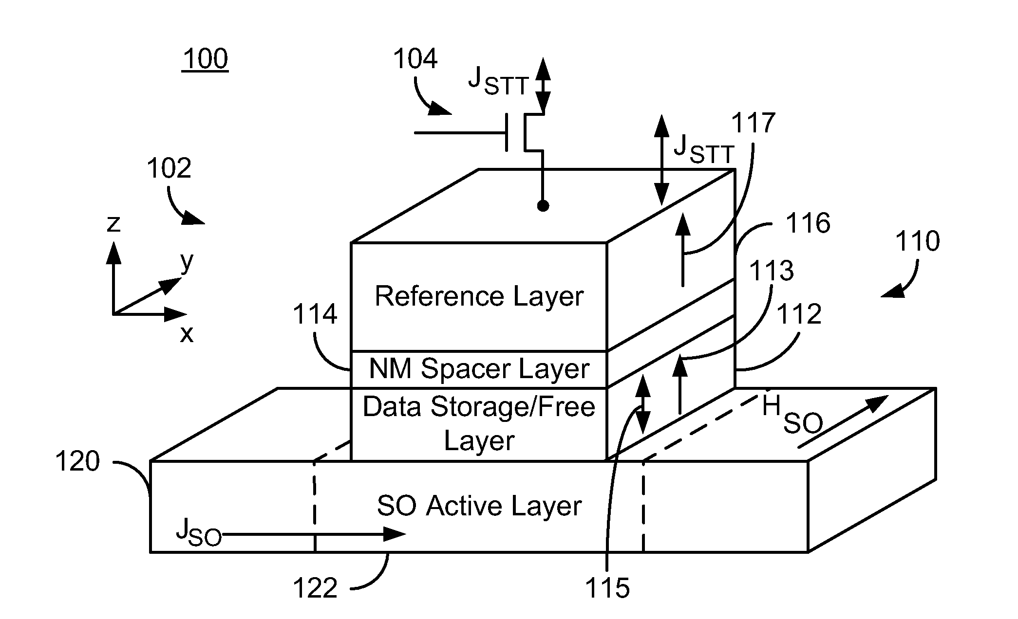
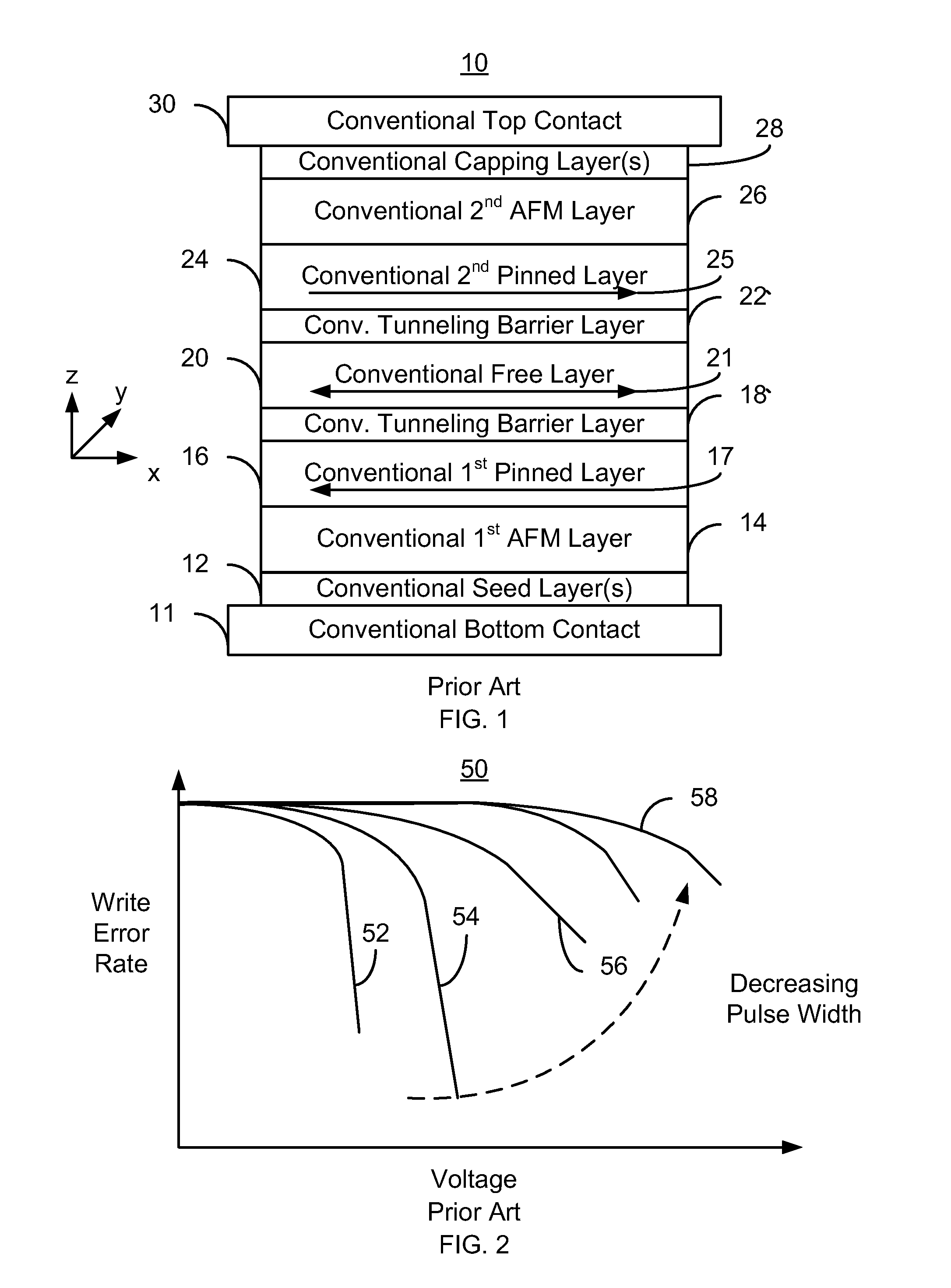
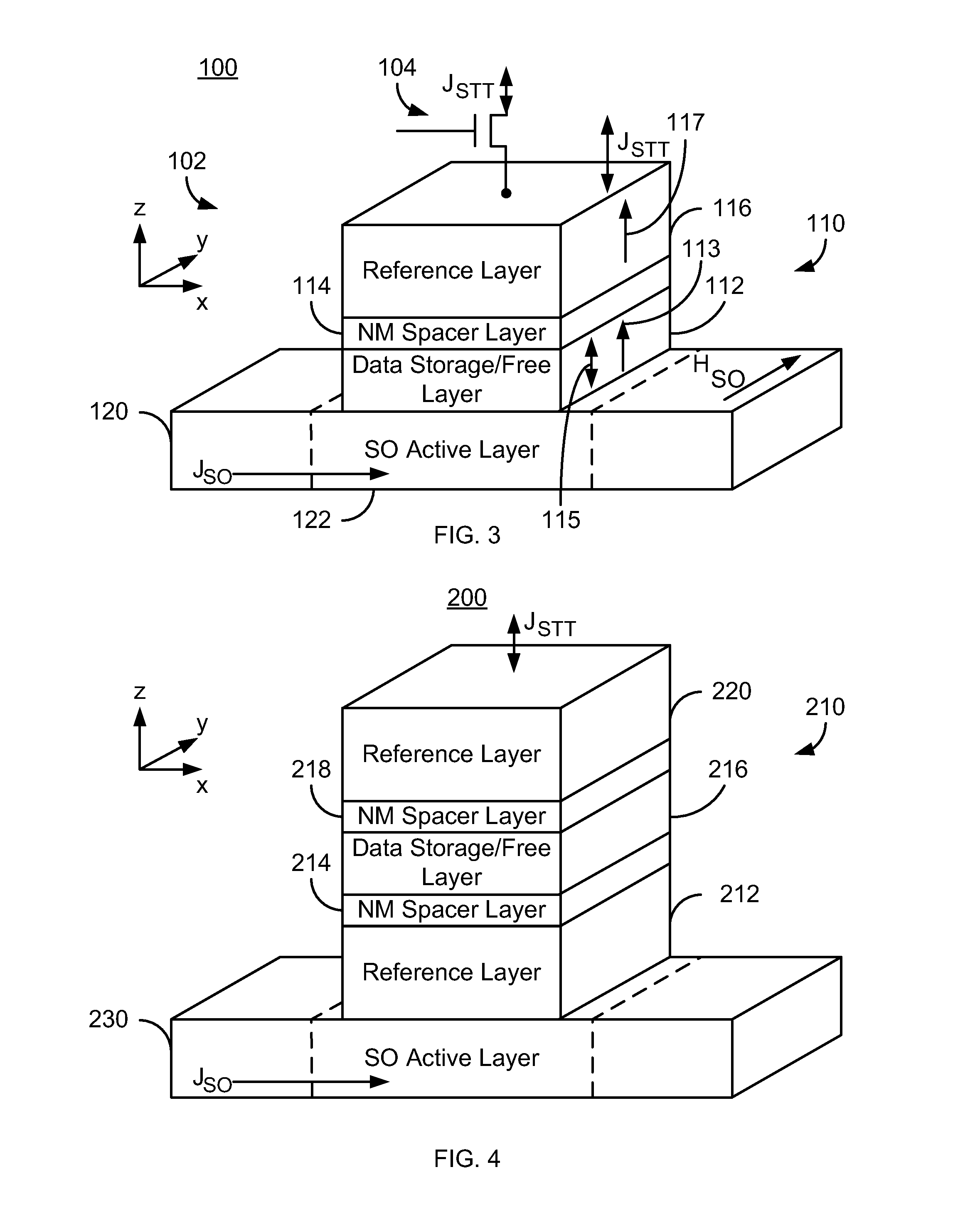
[0030]The exemplary embodiments relate to magnetic junctions usable in magnetic devices, such as magnetic memories, and the devices using such magnetic junctions. The following description is presented to enable one of ordinary skill in the art to make and use the invention and is provided in the context of a patent application and its requirements. Various modifications to the exemplary embodiments and the generic principles and features described herein will be readily apparent. The exemplary embodiments are mainly described in terms of particular methods and systems provided in particular implementations. However, the methods and systems will operate effectively in other implementations. Phrases such as “exemplary embodiment”, “one embodiment” and “another embodiment” may refer to the same or different embodiments as well as to multiple embodiments. The embodiments will be described with respect to systems and / or devices having certain components. However, the systems and / or devi...


PUM


Abstract

A magnetic memory is described. The magnetic memory includes dual magnetic junctions and spin-orbit interaction (SO) active layer(s). Each dual magnetic junction includes first and second reference layers, first and second nonmagnetic spacer layers and a free layer. The free layer is magnetic and between the nonmagnetic spacer layers. The nonmagnetic spacer layers are between the corresponding reference layers and the free layer. The SO active layer(s) are adjacent to the first reference layer of each dual magnetic junction. The SO active layer(s) exert a SO torque on the first reference layer due to a current passing through the SO active layer(s) substantially perpendicular to a direction between the SO active layer(s) and the first reference layer. The first reference layer has a magnetic moment changeable by at least the SO torque. The free layer is switchable using a spin transfer write current driven through the dual magnetic junction.

Description

CROSS-REFERENCE TO RELATED APPLICATIONS[0001]This application claims the benefit of provisional Patent Application Ser. No. 61 / 785,682, filed Mar. 14, 2013, entitled METHOD AND SYSTEM FOR PROVIDING INVERTED DUAL MAGNETIC TUNNELING JUNCTIONS USING SPIN-ORBIT INTERACTION-BASED SWITCHING AND MEMORIES UTILIZING THE DUAL MAGNETIC TUNNELING JUNCTIONS, assigned to the assignee of the present application, and incorporated herein by reference. This application is a continuation in-part of U.S. patent application Ser. No. 13 / 594,824, field Aug. 26, 2012, entitled METHOD AND SYSTEM FOR PROVIDING A MAGNETIC TUNNELING JUNCTION USING SPIN-ORBIT INTERACTION BASED SWITCHING AND MEMORIES UTILIZING THE MAGNETIC TUNNELING JUNCTION, assigned to the assignee of the present application, and incorporated herein by reference.BACKGROUND OF THE INVENTION[0002]Magnetic memories, particularly magnetic random access memories (MRAMs), have drawn increasing interest due to their potential for high read / write spee...

Claims


Application Information

Patent Timeline
Patent Type & Authority Applications(United States)
IPC IPC(8): H01L43/02G11C11/16H01L43/12
CPCH01L43/02G11C11/16H01L43/12H01F10/3263H01F10/3286H01F10/329H01F41/325G11C11/18G11C11/1659G11C11/161G11C11/1675H10B61/22H10N50/80H10N50/10H10N50/01
Inventor KHVALKOVSKIY, ALEXEY VASILYEVITCHAPALKOV, DMYTROKROUNBI, MOHAMAD TOWFIK
Owner SAMSUNG ELECTRONICS CO LTD
Why Eureka
Try Eureka