Radiation detection panel, radiation imaging device, and diagnostic imaging device

a radiation detection panel and detection panel technology, applied in the field of radiation, can solve the problems of troublesome storage of data after imaging data and complicated process, and achieve the effect of accurate imaging data

Active Publication Date: 2014-02-27
SEMICON ENERGY LAB CO LTD
View PDF3 Cites 14 Cited by
  • Summary
  • Abstract
  • Description
  • Claims
  • Application Information

AI Technical Summary

Benefits of technology

[0015]In a conversion unit (e.g., a scintillator) of a radiation detection panel with indirect conversion, there occurs a phenomenon in which light emission continues even after radiation emission stops (which is called afterglow). However, when an interval long enough to sufficiently reduce afterglow is provided between stop of radiation emission (A1 in FIG. 11A) and the next radiation emission (A2 in FIG. 11A) as shown in FIG. 11A, for example, adverse effect of afterglow on a signal output from a detection circuit can be reduced.
[0049]With the use of the radiation detection panel in a radiation imaging device, the radiation imaging device can obtain accurate imaging data.

Problems solved by technology

In the case of employing a photographic film, a method of digitizing imaging data is commonly used because storage of photographic films, that is, storage of data after imaging is troublesome.
Although imaging data can be digitized by the method, the process is complicated because an image is first obtained as analog data by the imaging plate and then is digitized by the bio-imaging analyzer.

Method used


Image

  • Radiation detection panel, radiation imaging device, and diagnostic imaging device
  • Radiation detection panel, radiation imaging device, and diagnostic imaging device
  • Radiation detection panel, radiation imaging device, and diagnostic imaging device

Examples


embodiment 1

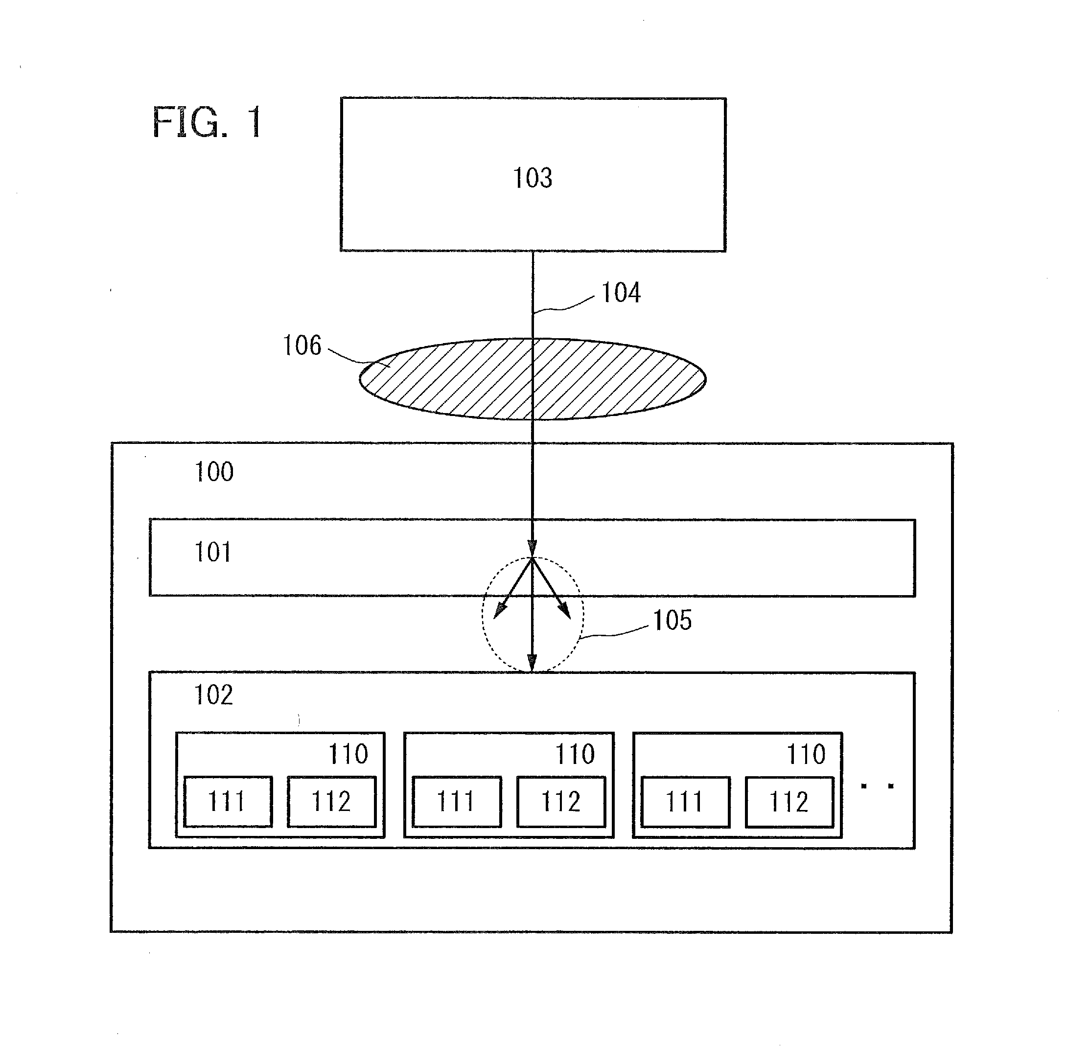
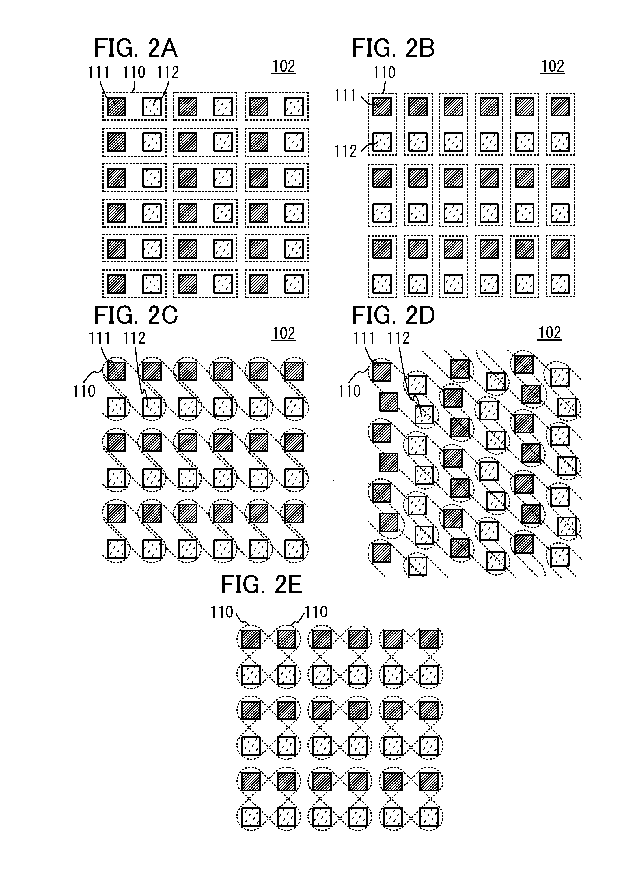
[0068]In Embodiment 1, the structure of a radiation detection panel will be described with reference to FIG. 1 and FIGS. 2A to 2E.

[0069]An overview of the structure of a radiation detection panel will be described with reference to FIG. 1. In FIG. 1, a radiation detection panel 100 includes a conversion unit 101 that receives radiation 104 emitted from the outside and converts the radiation 104 into light, and a plurality of detection circuits 110 each including a first output circuit 111 and a second output circuit 112 each of which outputs a signal based on light 105 emitted from the conversion unit 101. Note that the radiation 104 is emitted from a radiation source 103 and enters the radiation detection panel 100. An object 106 is disposed between the radiation detection panel 100 and the radiation source 103.

[0070]The conversion unit 101 includes a substance that absorbs energy of incident radiation (e.g., X-rays, y-rays, n-rays, or neutron rays) and emits light (e.g., infrared ...

embodiment 2

[0145]Embodiment 2 shows examples of the structure of an integrator circuit used to be connected to the fourth wiring 314 (OUT).

[0146]FIG. 6A illustrates an integrator circuit including an operational amplifier circuit (also referred to as an op-amp). An inverting input terminal of the operational amplifier circuit is connected to the fourth wiring 314 (OUT) through a resistor R. A non-inverting input terminal of the operational amplifier circuit is grounded. An output terminal of the operational amplifier circuit is connected to the inverting input terminal of the operational amplifier circuit through a capacitor C.

[0147]Here, the operational amplifier circuit is assumed to be an ideal operational amplifier circuit. In other words, it is assumed that input impedance is infinite (the input terminals draw no current). Since the potential of the non-inverting input terminal and the potential of the inverting input terminal are equal in a steady state, the potential of the inverting in...

embodiment 3

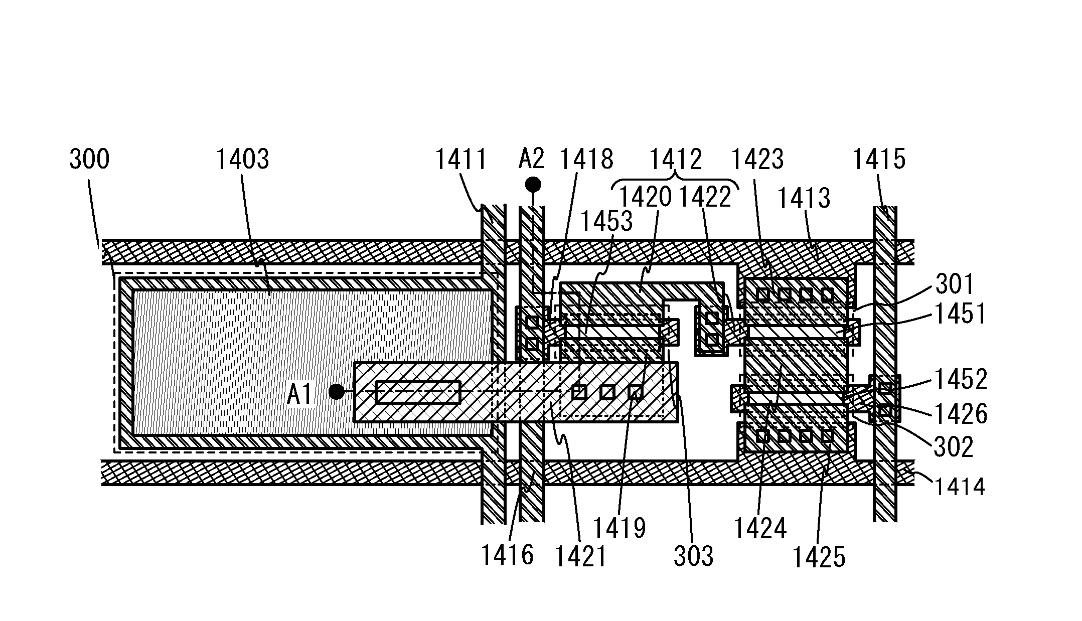
[0157]In Embodiment 3, the configuration and operation flow of the detection circuit 110 including the first output circuit 111 and the second output circuit 112, which are different from those in Embodiment 1, will be described with reference to FIGS. 7A and 7B, FIG. 8, FIGS. 9A and 9B, and FIG. 10.

1)>The detection circuit 110 including the first output circuit 111 and the second output circuit 112 may have a configuration illustrated in FIG. 7A. Although the components of the detection circuit in FIG. 7A are the same as those in FIG. 3A, the configuration in FIG. 7A differs from that in FIG. 3A in that one electrode of the photoelectric conversion element 300 is electrically connected to one of the source and the drain of the third transistor 303 and the other electrode of the photoelectric conversion element 300 is electrically connected to the first wiring 311 (PR).

[0158]Note that as described in Embodiment 1, it is possible to employ any of the following structures: a capacitor...


PUM


Abstract

To achieve a radiation detection panel capable of outputting a signal for generating an accurate pixel signal regardless of the performance of a conversion unit, a detection circuit that outputs a signal used for generating a pixel signal includes a first output circuit that outputs a signal due to afterglow, and a second output circuit that outputs a signal including both a signal based on radiation emission and a signal due to afterglow. Transistors using an oxide semiconductor material for a channel formation region are used as some transistors included in the first and second output circuits. In the radiation detection panel having this structure, the signal (a first signal or a second signal) can be held in each output circuit; therefore, after all output circuits hold the signal (the first signal or the second signal), the first signal and the second signal can be sequentially output from detection circuits.

Description

BACKGROUND OF THE INVENTION[0001]1. Field of the Invention[0002]The present invention relates to a radiation detection panel and a radiation imaging device including the radiation detection panel. The radiation imaging device particularly relates to a diagnostic imaging device in which a radiation source can emit X-rays.[0003]2. Description of the Related Art[0004]A device that images an object with radiation (hereinafter referred to as a radiation imaging device) is used in various applications in medical and industrial fields; for example, in the medical field, a diagnostic imaging device that images the inside of a human body with X-rays is widely used in medical practice.[0005]With a conventional diagnostic imaging device using X-rays, an X-ray source emits X-rays to a specific part (e.g., a bone or a lung) of a patient, and X-rays passing through the part are projected on a photographic film or the like. Then, the photographic film is developed, so that the inside of the specif...

Claims


Application Information

Patent Timeline
Patent Type & Authority Applications(United States)
IPC IPC(8): A61B6/00
CPCA61B6/4208G01T1/20G01T1/208H04N5/32H04N25/63H04N25/75
Inventor KUROKAWA, YOSHIYUKIIKEDA, TAKAYUKI
Owner SEMICON ENERGY LAB CO LTD
Why Eureka
Try Eureka