Method of forming single-mode polymer waveguide array connector

a polymer waveguide and array connector technology, applied in the field of waveguides, can solve the problems of accumulating coupling losses and coupling losses of ferrules

Inactive Publication Date: 2014-03-06
IBM CORP
View PDF5 Cites 19 Cited by
  • Summary
  • Abstract
  • Description
  • Claims
  • Application Information

AI Technical Summary

Benefits of technology

[0031]An object of the present invention is to provide a method of forming a single-mode polymer waveguide array connector that can provide precise alignment of a plurality of cores of polymer waveguide arrays when the polymer waveguide array conn

Problems solved by technology

Otherwise, the positioning error directly leads to a coupling loss.
In addition, as more ferrules are

Method used


Image

  • Method of forming single-mode polymer waveguide array connector
  • Method of forming single-mode polymer waveguide array connector
  • Method of forming single-mode polymer waveguide array connector

Examples


Embodiment Construction

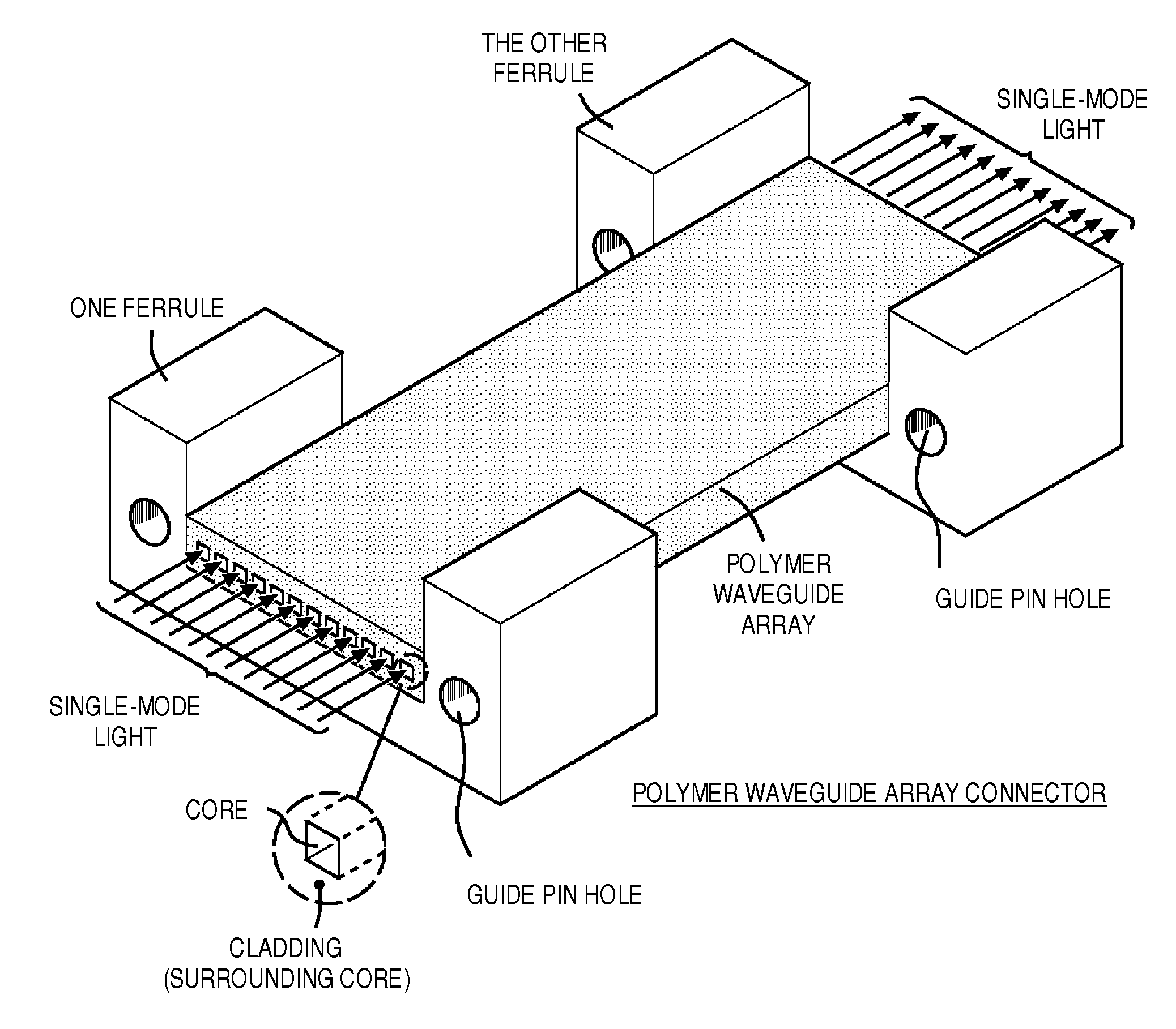
[0044]The disclosure describes a characteristic method of forming a single-mode polymer waveguide array connector that can provide precise alignment of a plurality of cores of polymer waveguide arrays when the polymer waveguide array connector is connected to another polymer waveguide array connector or provide precise alignment of a plurality of cores of a polymer waveguide array and a fiber array when the single-mode polymer waveguide array connector is connected to a single-mode fiber array connector.

[0045]FIG. 4 is a perspective view for illustrating a combination of a plurality of molds (a first mold (A) and a second mold (B)) used in a partial process of a plurality of processes of forming a single-mode polymer waveguide array connector.

[0046]The first mold (A) has a plurality of ridges (projections) formed on a surface thereof, the ridges being intended to shape a plurality of cores of a waveguide array.

[0047]The second mold (B) is to be combined with the first mold (A) and h...


PUM

PropertyMeasurementUnit
Fractionaaaaaaaaaa
Fractionaaaaaaaaaa
Lengthaaaaaaaaaa

Abstract

A method of forming a single-mode polymer waveguide array connector that provides precise alignment of a plurality of cores of polymer waveguide arrays with respect to an absolute reference position, such as a guide pin hole in a ferrule, when the polymer waveguide array connector is connected to another polymer waveguide array connector or provides precise alignment of a plurality of cores of a polymer waveguide array and a fiber array with respect to the absolute reference position when the polymer waveguide array connector is connected to a single-mode fiber array connector. A plurality of cores of single-mode polymer waveguide arrays or single-mode fiber arrays is precisely aligned with each other. In addition, there is provided a combination of a plurality of molds, e.g., a first mold (A) and a second mold (B), used in a plurality of processes in a specific method.

Description

CROSS-REFERENCE TO RELATED APPLICATION[0001]This application is based upon and claims priority from prior Japanese patent application number 2012-194909, filed Sep. 5, 2012, the entire contents of which are hereby incorporated by reference herein.BACKGROUND OF THE INVENTION[0002]1. Field of the Invention[0003]This invention relates generally to waveguides, and more specifically to a method of forming a single-mode polymer waveguide array connector.[0004]2. Description of the Related Art[0005]In the field of building of an optical interconnection system, a polymer waveguide is attracting attention. Compared with an approach involving arranging and fixing a plurality of fibers in an array, the polymer waveguide can provide a more inexpensive optical signal channel with higher reliability because an integrated polymer waveguide array can be formed in a process using the polymer material.[0006]FIG. 1 is a perspective view for illustrating a configuration of a single-mode polymer wavegui...

Claims


Application Information

Patent Timeline
IPC IPC(8): G02B6/38
CPCG02B6/3865G02B6/3885G02B6/10G02B6/138B29D11/0075B29K2995/0027B29D11/00721B29C33/424B29D11/00663G02B6/448G02B6/4231B29C35/0888B29C43/021B29C43/184G02B6/4403
Inventor NUMATA, HIDETOSHITOKUNARI, MASAO
Owner IBM CORP
Why Eureka
Try Eureka