Patterning method for oleds

a technology of oleds and patterns, applied in the direction of basic electric elements, electrical apparatus, semiconductor devices, etc., can solve the problems of broken processing windows, achieve ultra-rapid growth, rapid printing of large-scale electronics, and break the processing window

Active Publication Date: 2014-03-06
UNIVERSAL DISPLAY
View PDF2 Cites 61 Cited by
  • Summary
  • Abstract
  • Description
  • Claims
  • Application Information

AI Technical Summary

Benefits of technology

[0017]One unique aspect of OVJP is that the organic species may be accelerated by the flow of a much lighter carrier gas to hyperthermal velocities. This can lead to denser and more ordered thin films, which potentially broadens the processing window for ultra-rapid growth of high quality thin films for device applications. This acceleration may also allow the instantaneous local deposition rate of OVJP to exceed that of the alternative broad-area deposition methods, resulting in an advantage in the rapid printing of large-scale electronics.
[0018]Because OVJP does not use liquid solvents, it may allo

Problems solved by technology

This can lead to denser and more ordered thin films, which potentially broadens the proc

Method used


Image

  • Patterning method for oleds
  • Patterning method for oleds
  • Patterning method for oleds

Examples


first embodiment

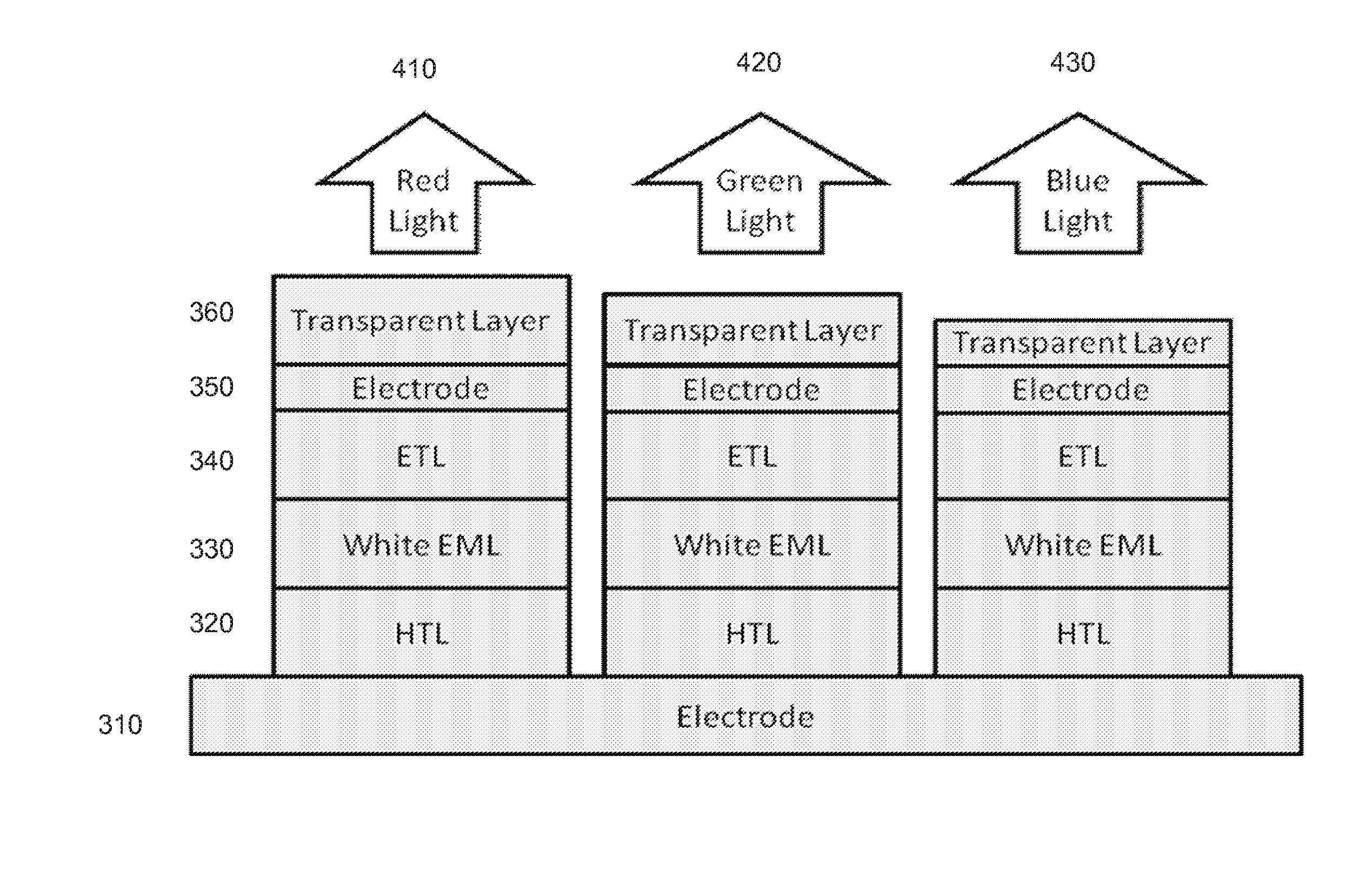
[0099]A first embodiment is described with reference to FIG. 3: A substrate / first electrode 310 may be loaded into an OVJP chamber. An HTL 320 (and / or an HIL) may be deposited using OVJP so that a first thickness of HTL and / or HIL is deposited on a first set of sub-pixels 410. A second thickness of HIL and / or HTL may be deposited on a second set of sub-pixels 420. A third thickness of HIL and / or HTL may be deposited on a third set of sub-pixels 430. In this example, and the others that follow, the “first thickness,”“second thickness” and “third thickness” are to be understood as different thicknesses, i.e. including a difference that is intended, and is typically greater than the mere processing imperfections in deposited layers that are otherwise intended to be the same thickness. For example, the first thickness, second thickness and third thickness may include differences greater than approximately 5 Å, approximately 10 Å, or approximately 20 Å. The different thicknesses may alte...

second embodiment

[0104]A second embodiment is described with reference to FIG. 4: HIL and / or HTL 320 and EML 330 may all be deposited on sets of sub-pixels 410, 420, 430, conventionally using VTE and (optionally) shadow masks (the shadow mask being optionally used if different thicknesses and / or compositions are used for different sub-pixels). The substrate may be subsequently loaded into an OVJP chamber, and a first thickness of ETL 340 is deposited on a first set of subpixels 410 and a second thickness of ETL 340 is deposited on a second set of sub-pixels 420. A third thickness of ETL 340 may be deposited on a third set of sub-pixels 430.

[0105]A second electrode 350 may be deposited, for example, using conventional VTE.

third embodiment

[0106]A third embodiment is described with reference to FIG. 5. A first thickness of HIL and / or HTL 320 is deposited on a first set of sub-pixels 410 and a second thickness of HIL and / or HTL 320 is deposited on a second set of sub-pixels 420, e.g. using OVJP. A third thickness of HIL and / or HTL 320 may be deposited on a third set of sub-pixels 430, e.g. by OVJP.

[0107]An EML 330 may then be deposited, e.g. OVJP, or other techniques. Optionally, a different EML may be deposited on each set of sub-pixels 410, 420, 430, such as a Red EML, a Green EML and a Blue EML. Of note, the EML 330 in FIG. 5 may have the same or different thicknesses.

[0108]A first thickness of ETL 340 is deposited on the first set of sub-pixels 410, and a second thickness of ETL 340 is deposited on the second set of sub-pixels 420 also using OVJP. A third thickness of ETL 340 may be deposited on the third set of sub-pixels 430, e.g. by OVJP. Thus, the device shown in FIG. 5 may have multiple layers including differ...


PUM


Abstract

Methods of fabricating a device having laterally patterned first and second sub-devices, such as subpixels of an OLED, are provided. Exemplary methods may include depositing via organic vapor jet printing (OVJP) a first organic layer of the first sub-device and a first organic layer of the second sub-device. The first organic layer of the first sub-device and the first organic layer of the second sub-device are both the same type of layer, but have different thicknesses. The type of layer is selected from an ETL, an HTL, an HIL, a spacer and a capping layer.

Description

FIELD OF THE INVENTION[0001]The present invention relates to methods of producing organic light emitting devices, and more specifically to manufacturing processes for providing layer thicknesses for microcavity optimization without the use of a shadow mask.BACKGROUND[0002]Opto-electronic devices that make use of organic materials are becoming increasingly desirable for a number of reasons. Many of the materials used to make such devices are relatively inexpensive, so organic opto-electronic devices have the potential for cost advantages over inorganic devices. In addition, the inherent properties of organic materials, such as their flexibility, may make them well suited for particular applications such as fabrication on a flexible substrate. Examples of organic opto-electronic devices include organic light emitting devices (OLEDs), organic phototransistors, organic photovoltaic cells, and organic photodetectors. For OLEDs, the organic materials may have performance advantages over c...

Claims


Application Information

Patent Timeline
IPC IPC(8): H01L51/56
CPCH10K59/30H10K59/35H10K71/16H10K71/135H10K50/11H10K2101/40H10K50/125H10K50/156H10K50/166H10K50/17H10K50/8428H10K50/852H10K50/844H10K2102/351H10K71/00H10K50/15H10K50/16H10K59/32H10K59/1201H10K2101/10
Inventor HARIKRISHNA MOHAN, SIDDHARTHBURROWS, PAUL E.BROWN, JULIA J.
Owner UNIVERSAL DISPLAY
Why Eureka
Try Eureka