Method for manufacturing silicon carbide semicondutor device having trench gate structure

a semiconductor device and trench gate technology, applied in the direction of semiconductor devices, basic electric elements, electrical equipment, etc., can solve the problems of insufficient concentration, gate insulation film damage at a corner of the trench, and difficulty, so as to improve the process window for forming the trench

Inactive Publication Date: 2009-12-17
DENSO CORP
View PDF3 Cites 28 Cited by
  • Summary
  • Abstract
  • Description
  • Claims
  • Application Information

AI Technical Summary

Benefits of technology

[0009]In the above method, the deep layer is formed at a deep position, and therefore, a gap between the bottom of the deep layer and a bottom of the trench can be increased. A process window for forming the trench is improved.
[0011]In the above method, the deep layer is formed at a deep position, and therefore, a gap between the bottom of the deep layer and a bottom of the trench can be increased. A process window for forming the trench is improved.
[0013]In the above method, the deep layer is formed at a deep position, and therefore, a gap between the bottom of the deep layer and a bottom of the trench can be increased. A process window for forming the trench is improved.
[0015]In the above method, the deep layer is formed at a deep position, and therefore, a gap between the bottom of the deep layer and a bottom of the trench can be increased. A process window for forming the trench is improved.

Problems solved by technology

However, when the SiC device has the trench gate structure, a difficulty may arise.
Thus, the gate insulation film at a corner of the trench may be damaged.
However, the concentration is not sufficiently reduced, and thereby, it is necessary to reduce the electric field concentration much more.

Method used


Image

  • Method for manufacturing silicon carbide semicondutor device having trench gate structure
  • Method for manufacturing silicon carbide semicondutor device having trench gate structure
  • Method for manufacturing silicon carbide semicondutor device having trench gate structure

Examples


first embodiment

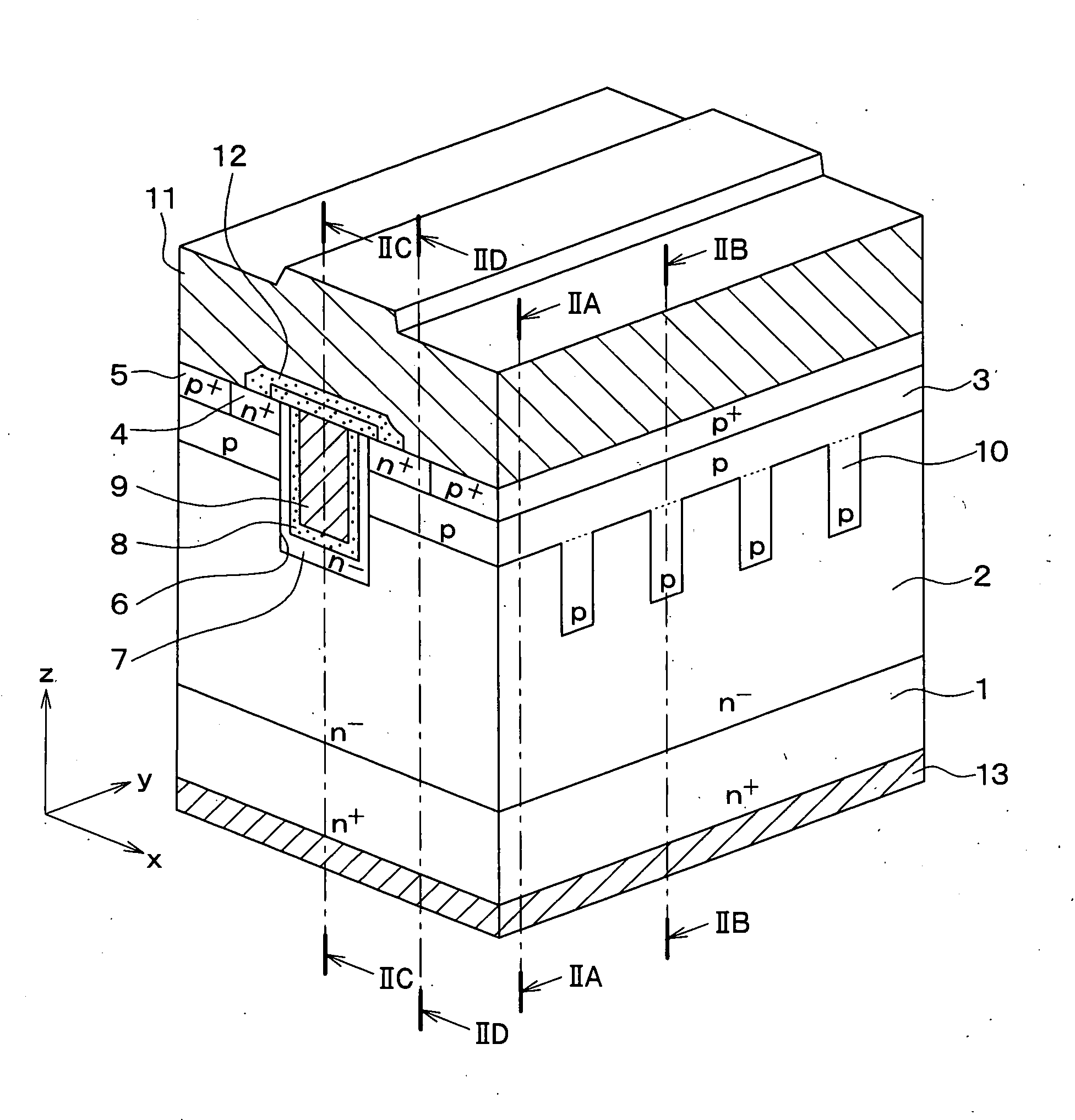
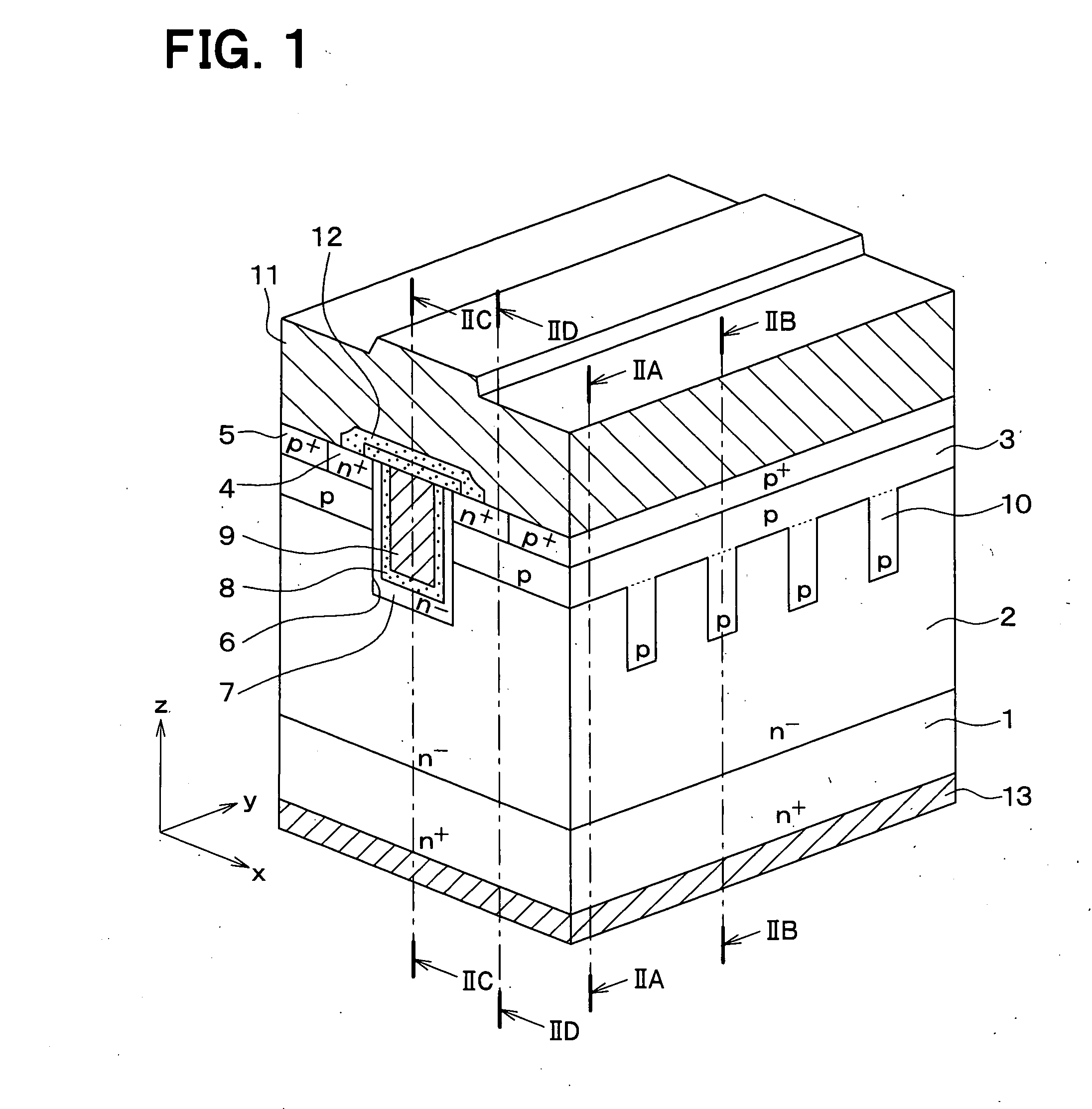
[0044]In view of the above requirement, a SiC semiconductor device according to a first embodiment is proposed. The device is an accumulation type trench gate MOSFET.

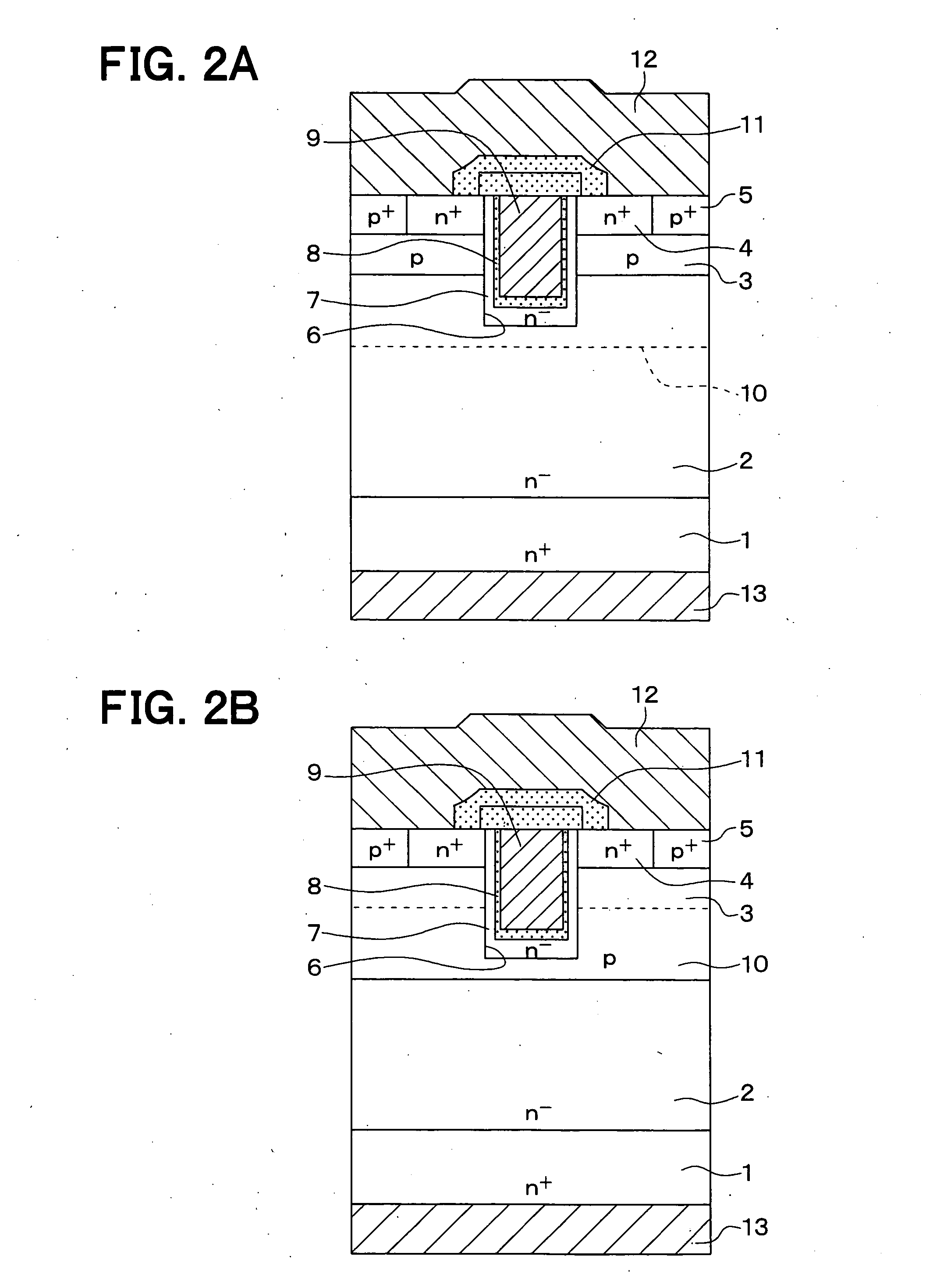
[0045]FIG. 1 shows a part of a MOSFET having a trench gate structure. The part corresponds to one cell in the MOSFET. Although FIG. 1 shows the one cell in the MOSFET, the MOSFET includes multiple cells, which are arranged adjacently along with a line. FIG. 2A shows a cross section of the MOSFET taken along line IIA-IIA in FIG. 1. Specifically, the cross section of FIG. 2A is taken along a X-Z plane passing through the line IIA-IIA in FIG. 1. FIG. 2B shows a cross section of the MOSFET taken along line IIB-IIB in FIG. 1. Specifically, the cross section of FIG. 2B is taken along a X-Z plane passing through the line IIB-IIB in FIG. 1. FIG. 2C shows a cross section of the MOSFET taken along line IIC-IIC in FIG. 1. Specifically, the cross section of FIG. 2C is taken along a Y-Z plane passing through the line IIC-IIC in FIG....

second embodiment

[0091]In a SiC semiconductor device according to a second embodiment, an on-state resistance is reduced.

[0092]FIG. 7 shows the SiC semiconductor device having a trench gate structure. FIG. 8A shows a cross section of the MOSFET taken along line VIIIA-VIIIA in FIG. 7. Specifically, the cross section of FIG. 8A is taken along a X-Z plane passing through the line VIIIA-VIIIA in FIG. 7. FIG. 8B shows a cross section of the MOSFET taken along line VIIIB-VIIIB in FIG. 7. Specifically, the cross section of FIG. 8B is taken along a X-Z plane passing through the line VIIIB-VIIIB in FIG. 7. FIG. 8C shows a cross section of the MOSFET taken along line VIIIC-VIIIC in FIG. 7. Specifically, the cross section of FIG. 8C is taken along a Y-Z plane passing through the line VIIIC-VIIIC in FIG. 7. FIG. 8D shows a cross section of the MOSFET taken along line VIIID-VIIID in FIG. 7. Specifically, the cross section of FIG. 8D is taken along a Y-Z plane passing through the line VIIID-VIIID in FIG. 7.

[0093]...

third embodiment

[0099]A SiC semiconductor device according to a third embodiment is similar to the device in FIG. 7. Specifically, the device in the present embodiment, the on-state resistance is reduced.

[0100]In the second embodiment, the device includes the current dispersion layer 30. However, the deep layer 10 is separated from the base region 3 with the current dispersion layer 30, so that the deep layer 10 becomes a floating state. Accordingly, the effect of the electric field relaxation is small, compared with a case where the deep layer 10 contacts the base region 3, and the electric potential of the deep layer 10 is fixed to the source potential. In view of this point, in the third embodiment, the on-state resistance of the device is improved.

[0101]FIG. 11 shows the SiC semiconductor device having a trench gate structure. FIG. 12A shows a cross section of the MOSFET taken along line XIIA-XIIA in FIG. 11. Specifically, the cross section of FIG. 12A is taken along a X-Z plane passing through...


PUM

PropertyMeasurementUnit
offset angleaaaaaaaaaa
electric fieldaaaaaaaaaa

Abstract

A manufacturing method of a SiC device includes: forming a drift layer on a substrate having an orientation tilted from a predetermined orientation with an offset angle; obliquely implanting a second type impurity with a mask on the drift layer so that a deep layer is formed in the drift layer, wherein the impurity is implanted to cancel the offset angle; forming a base region on the deep layer and the drift layer; implanting a first type impurity on the base region so that a high impurity source region is formed; forming a trench having a bottom shallower than the deep layer on the source region to reach the drift layer; forming a gate electrode in the trench via a gate insulation film; forming a source electrode on the source region and the base region; and forming a drain electrode on the substrate.

Description

CROSS REFERENCE TO RELATED APPLICATION[0001]This application is based on Japanese Patent Application No. 2008-157594 filed on Jun. 17, 2008, the disclosure of which is incorporated herein by reference.FIELD OF THE INVENTION[0002]The present invention relates to a method for manufacturing a silicon carbide semiconductor device having a trench gate structure.BACKGROUND OF THE INVENTION[0003]Recently, silicon carbide is well known as material for a power device having high electric field breakdown strength. Since a SiC semiconductor device has high electric field breakdown strength, the device can control large current. Accordingly, it is expected to apply the SiC semiconductor device to motor control for a motor in a hybrid vehicle.[0004]In the device, a channel density is increased so as to flow the large current. Here, in a silicon transistor, a trench gate type MOSFET is used for a large current device. The SiC semiconductor device may have trench gate structure. However, when the ...

Claims


Application Information

Patent Timeline
Patent Type & Authority Applications(United States)
IPC IPC(8): H01L21/336
CPCH01L21/26513H01L21/26586H01L29/045H01L29/0619H01L29/0623H01L29/7828H01L29/0847H01L29/1095H01L29/1608H01L29/66068H01L29/7813H01L29/0634
Inventor MIYAHARA, SHINICHIROUOKUNO, EIICHI
Owner DENSO CORP
Why Eureka
Try Eureka