MIM capacitor structure and method of fabrication

Active Publication Date: 2005-05-26
INFINEON TECH AG
View PDF27 Cites 26 Cited by
  • Summary
  • Abstract
  • Description
  • Claims
  • Application Information

AI Technical Summary

Benefits of technology

[0016] Advantages of embodiments of the present invention include reducing the number of masks required to manufacture a MIM capacitor, resulting in reduced processing costs. The at least one thin conductive material layer creates a smooth, defect-free planar top surface of a metallization layer. When a bottom plate is formed in the metallization layer having an improved surface, a MIM capacitor with improved reliability results.
[0017] The manufacturing methods described herein are compatible with aluminum back-end-of-the-line (BEOL) processes. Via interc

Problems solved by technology

Copper has a lower resistance and a higher conductivity than aluminum, but requires damascene processes and more expensive manufacturing processes.
Another problem with the prior art MIM capacitor 114 of FIG. 1 is that

Method used


Image

  • MIM capacitor structure and method of fabrication
  • MIM capacitor structure and method of fabrication
  • MIM capacitor structure and method of fabrication

Examples


Embodiment Construction

[0030] The making and using of the presently preferred embodiments are discussed in detail below. It should be appreciated, however, that the present invention provides many applicable inventive concepts that can be embodied in a wide variety of specific contexts. The specific embodiments discussed are merely illustrative of specific ways to make and use the invention, and do not limit the scope of the invention.

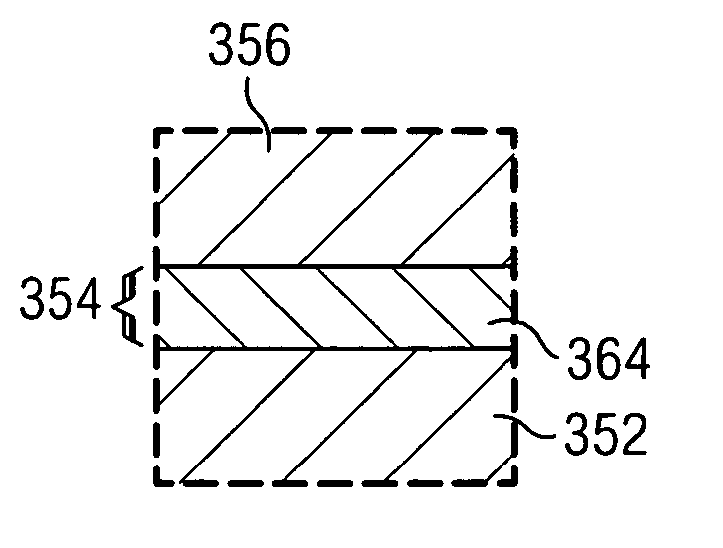
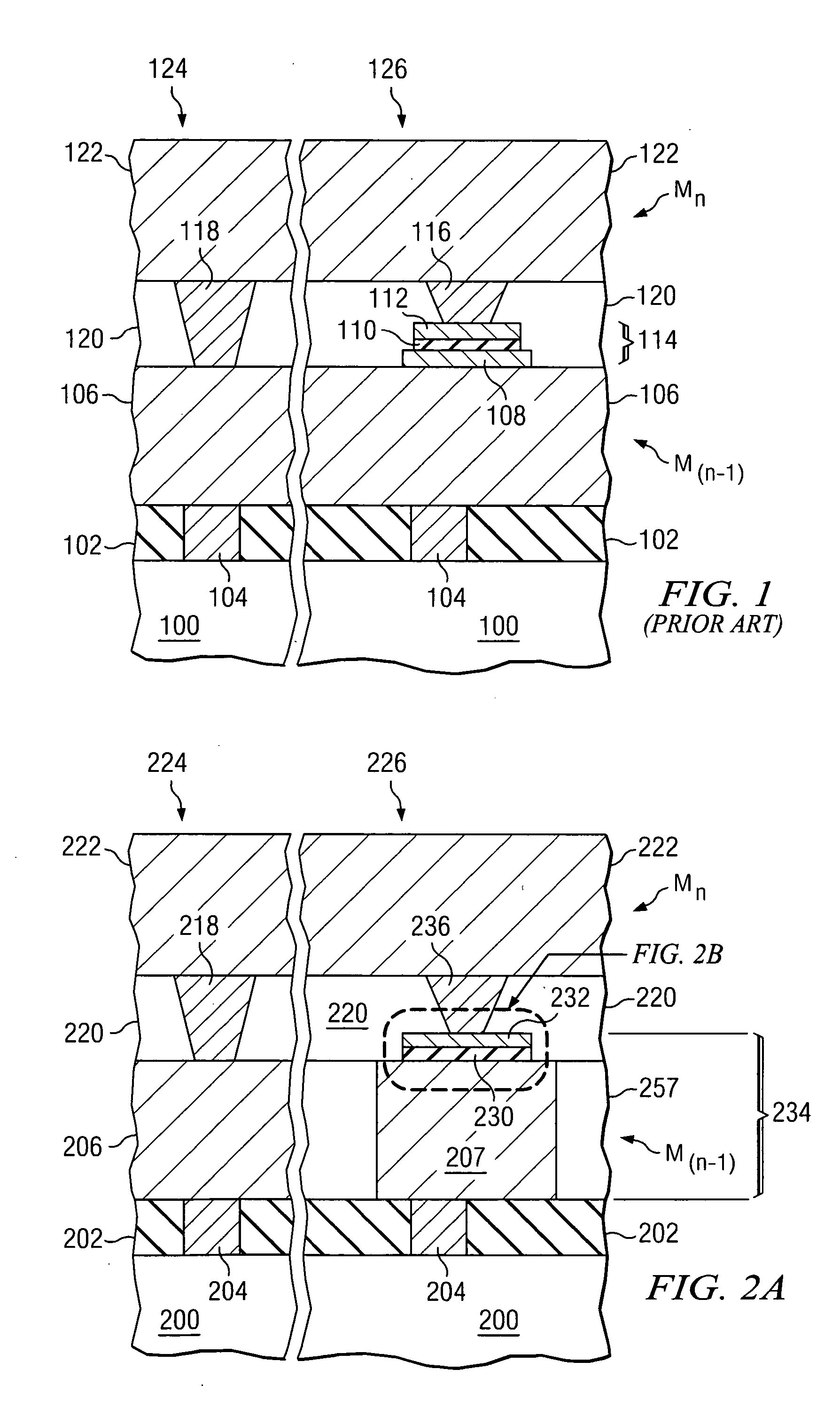
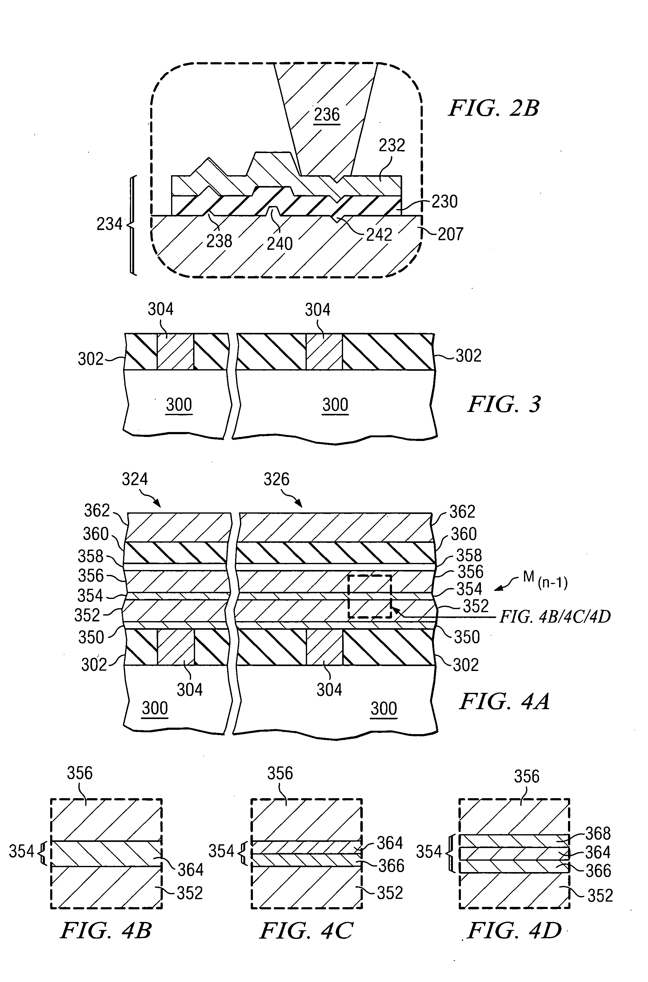
[0031]FIG. 2A shows a cross-sectional view of a preferred embodiment of the present invention, wherein a MIM capacitor is formed having a bottom plate that resides within an entire thickness of a metallization layer of a semiconductor device. First, a workpiece 200 is provided. The workpiece 200 preferably comprises a semiconductor substrate and may include active areas or device regions formed therein, not shown. The workpiece may include a semiconductor substrate comprising silicon or other semiconductor materials covered by an insulating layer, for example. The workpiece...


PUM


Abstract

A method of forming a metal-insulator-metal (MIM) capacitor wherein a plate of a MIM capacitor is formed in the entire thickness of a metallization layer of a semiconductor device. At least one thin conductive material layer is disposed within the material of the metallization layer to reduce the surface roughness of the metallization layer, thus improving the reliability of the MIM capacitor. The thin conductive material layer may comprise TiN, TaN, or WN and may alternatively comprise a barrier layer disposed over or under the TiN, TaN, or WN. One plate of the MIM capacitor is patterned using the same mask that is used to pattern conductive lines in a metallization layer, thus reducing the number of masks that are required to manufacture the MIM capacitor.

Description

TECHNICAL FIELD [0001] The present invention relates generally to the fabrication of semiconductor devices, and more particularly to the fabrication of metal-insulator-metal (MIM) capacitor structures. BACKGROUND [0002] Capacitors are elements that are used extensively in semiconductor devices for storing an electrical charge. Capacitors essentially comprise two conductive plates separated by an insulator. The capacitance, or amount of charge held by the capacitor per applied voltage, depends on a number of parameters such as the area of the plates, the distance between the plates, and the dielectric constant value of the insulator between the plates, as examples. Capacitors are used in filters, analog-to-digital converters, memory devices, control applications, and many other types of semiconductor devices. [0003] One type of capacitor is a MIM capacitor, which is frequently used in mixed signal devices and logic semiconductor devices, as examples. MIM capacitors are used to store ...

Claims


Application Information

Patent Timeline
IPC IPC(8): H01L21/02H01L23/522
CPCH01L23/5223H01L28/60H01L28/75H01L2924/0002H01L2924/00
Inventor KIM, SUN-OODEMM, ERNST
Owner INFINEON TECH AG
Why Eureka
Try Eureka