

Liquid crystal display device and fabrication method thereof
- Summary
- Abstract
- Description
- Claims
- Application Information
AI Technical Summary
Benefits of technology
Problems solved by technology
Method used
Image

Examples
Embodiment Construction
[0056]The liquid crystal display (LCD) and its fabrication method will now be described in detail with reference to the accompanying drawings.
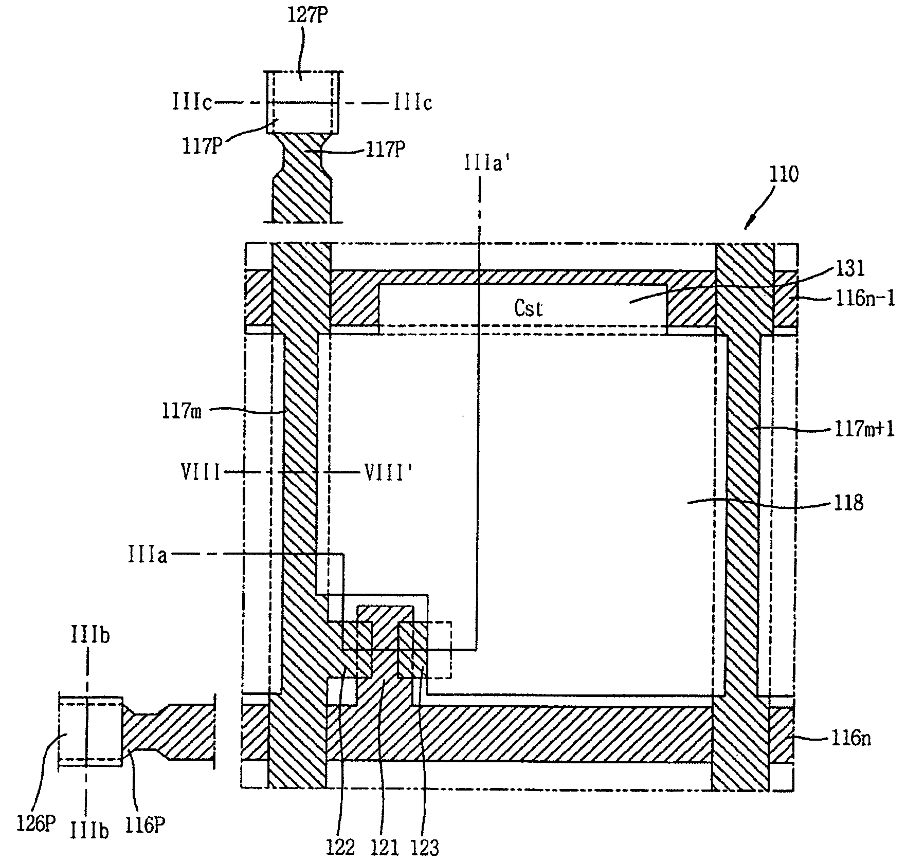
[0057]FIG. 4 is a plan view showing a portion of an array substrate of an LCD according to an exemplary embodiment of the present invention, in which a single pixel including a gate pad part and a data pad part is shown.
[0058]Actually, the N number of gate lines and M number of data lines are formed to cross each other to define the M×N number of pixels on the array substrate, and in order to simplify the explanation, only the single pixel is shown.
[0059]As shown, the nth gate line 116n and the mth data line are formed to be arranged vertically and horizontally to define the (m,n)th pixel region on the array substrate 110. A thin film transistor (TFT), a switching element, is formed at a crossing of the nth gate line 116n and the mth data line 117m. A pixel electrode 118 is formed within the pixel region and is connected with the TFT to drive ...
PUM
 Abstract
Description
Claims
Application Information