CMOS devices and manufacturing method thereof

Inactive Publication Date: 2019-02-14
GLOBALFOUNDRIES INC
View PDF9 Cites 6 Cited by
  • Summary
  • Abstract
  • Description
  • Claims
  • Application Information

AI Technical Summary

Benefits of technology

[0016]Separation of the formation of the sidewall spacers of the NFET and PFET transistors from the formation of the raised source and drain regions not only provides sidewall spacers of substantially identical thickness, but also reduces the number of masks required in the manufacturing process, and thereby simplifies the manufacturing process.
[0017]The simultaneous etch of the spacer layer with subsequent deposition of a sacrificial layer is compatible with both the formation of source and drain extensions and the formation of thick input/output spacers as they are required for I/O devices. As the sidewall spacers of the NFET and PFET transistors are etched at the same time, no additional steps with respect to the process of reference are needed for the formation of source and drain extensions. Rather, fewer masks are required, which makes t

Problems solved by technology

Unfortunately, very thin gate insulators have resulted in increased gate leakages or gate-induced leakages increasing circuit stand-by power for short transistor gate lengths.
Second, a very thin silicon layer creates the transistor channel.
The buried insulation (e.g., oxide) layer also constrains electrons flowing between the source and drain to significantly reduce performance and power-degrading leakage current.
In complementary metal-oxide-semiconductor (CMOS) devices comprising an N-type metal-oxide-semiconductor (NMOS) transistor and a P-type metal-oxide-semiconductor (PMOS) transistor, it has proven difficult in the past to manufacture sidewall spacers for the gate structures of th

Method used


Image

  • CMOS devices and manufacturing method thereof
  • CMOS devices and manufacturing method thereof
  • CMOS devices and manufacturing method thereof

Examples


Example

[0024]While the subject matter disclosed herein is susceptible to various modifications and alternative forms, specific embodiments thereof have been shown by way of example in the drawings and are herein described in detail. It should be understood, however, that the description herein of specific embodiments is not intended to limit the invention to the particular forms disclosed, but on the contrary, the intention is to cover all modifications, equivalents, and alternatives falling within the spirit and scope of the invention as defined by the appended claims.

DETAILED DESCRIPTION

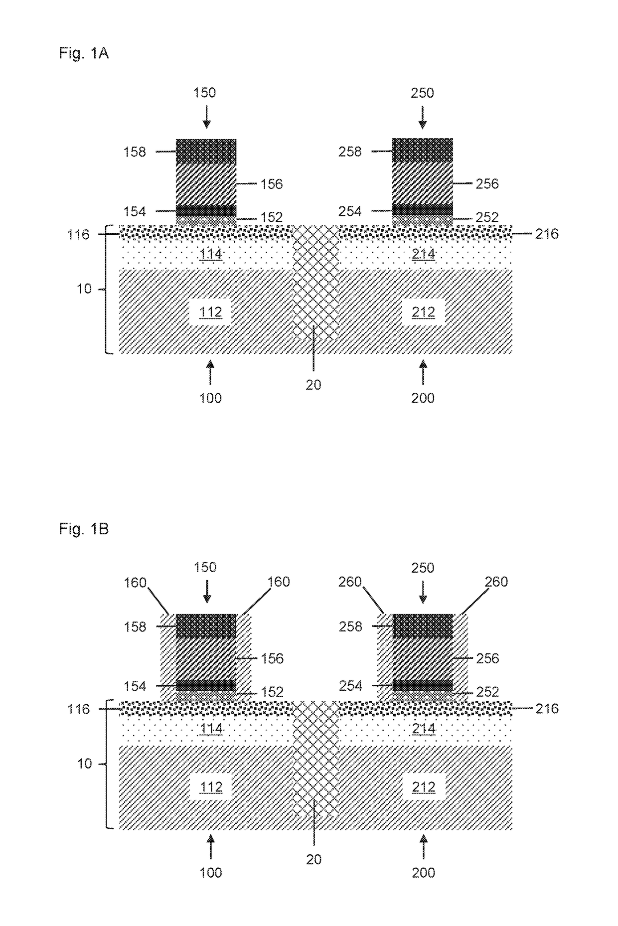
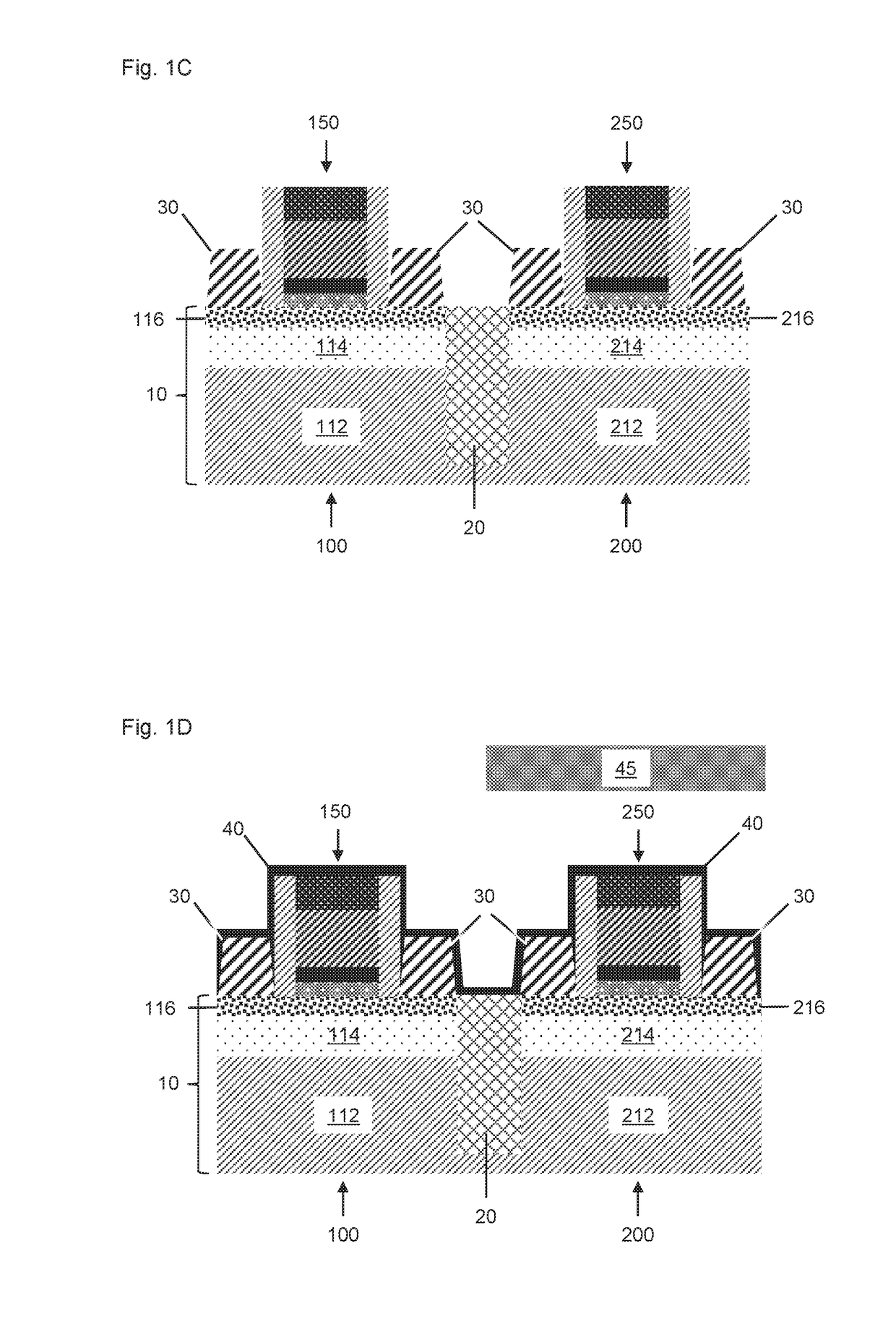
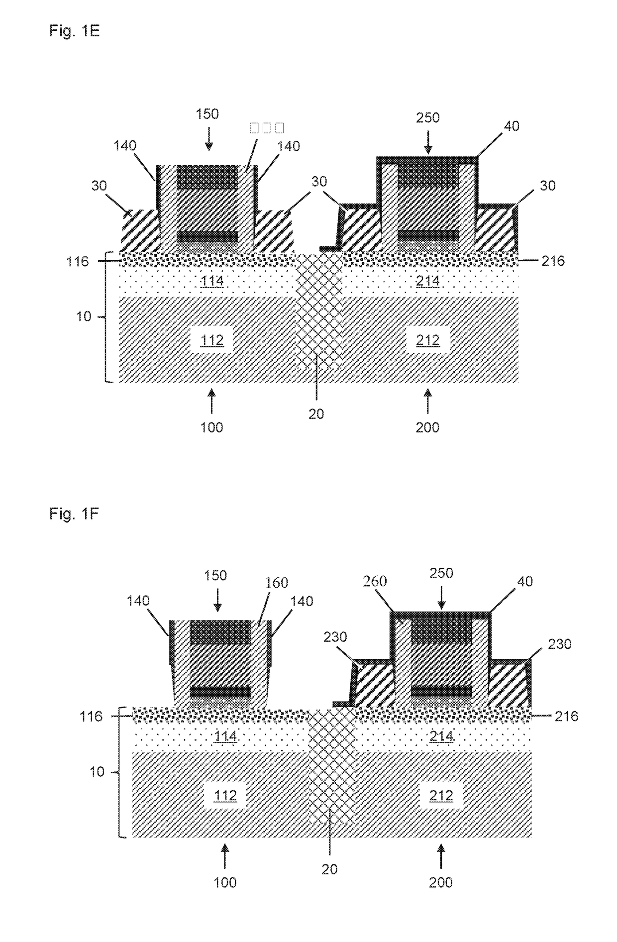
[0025]Various illustrative embodiments of the invention are described below. In the interest of clarity, not all features of an actual implementation are described in this specification. It will of course be appreciated that in the development of any such actual embodiment, numerous implementation-specific decisions must be made to achieve the developers' specific goals, such as compliance with system-rel...


PUM


Abstract

A method of manufacturing a complementary metal-oxide-semiconductor (CMOS) device comprising an N-type metal-oxide-semiconductor (NMOS) region and a P-type metal-oxide-semiconductor (PMOS) region is provided, that comprises: depositing a raised source and drain (RSD) layer of a first type in the NMOS region and the PMOS region at the same time; selectively removing the RSD layer of the first type in one of the NMOS region and the PMOS region; and depositing an RSD layer of a second type in the one of the NMOS region and the PMOS region.

Description

BACKGROUND1. Field of the Disclosure[0001]Generally, the subject matter disclosed herein relates to integrated circuits and particularly to transistor devices, in particular, field effect transistor devices with raised source and drain regions.2. Description of the Related Art[0002]As integrated circuits become more and more integrated, the sizes of the corresponding circuit elements, such as transistors, have to shrink accordingly. As a consequence, field effect transistors (FETs) with very thin gate dielectric layers using a high-k dielectric have been developed to mitigate short channel effects. Unfortunately, very thin gate insulators have resulted in increased gate leakages or gate-induced leakages increasing circuit stand-by power for short transistor gate lengths. As a remedy, sub-threshold leakage and other short channel effects have been controlled and reduced by thinning the device channel layer.[0003]Fully depleted (FD) devices have been formed in ultrathin silicon-on-ins...

Claims


Application Information

Patent Timeline
IPC IPC(8): H01L21/8238H01L27/092H01L21/8234
CPCH01L21/823807H01L21/823842H01L27/0925H01L2027/11822H01L21/823418H01L27/092H01L21/823857H01L21/823814H01L21/823864H01L29/41783H01L27/1203H01L21/84H01L29/4908H01L29/66628H01L29/6656
Inventor BAARS, PETERTHEES, HANS-JUERGENKAMMLER, THORSTEN
Owner GLOBALFOUNDRIES INC
Why Eureka
Try Eureka