Semiconductor structure and fabrication method thereof

Active Publication Date: 2010-02-04
NIKO SEMICON
View PDF3 Cites 1 Cited by
  • Summary
  • Abstract
  • Description
  • Claims
  • Application Information

AI Technical Summary

Benefits of technology

[0006]Therefore, it is a primary objective of the present invention to overcome the drawbacks of the prior art by reducing the number of masks needed for the semiconductor fabrication process. The present invention provides a semiconductor fabrication process which defines a plurality of separated spaces by us

Problems solved by technology

As the function of present integrated circuits becomes more powerful and the structure of the integrated circuits becomes more complicated, the number of masks needed for fabricating the integrated circuits increases acco

Method used


Image

  • Semiconductor structure and fabrication method thereof
  • Semiconductor structure and fabrication method thereof
  • Semiconductor structure and fabrication method thereof

Examples


Example

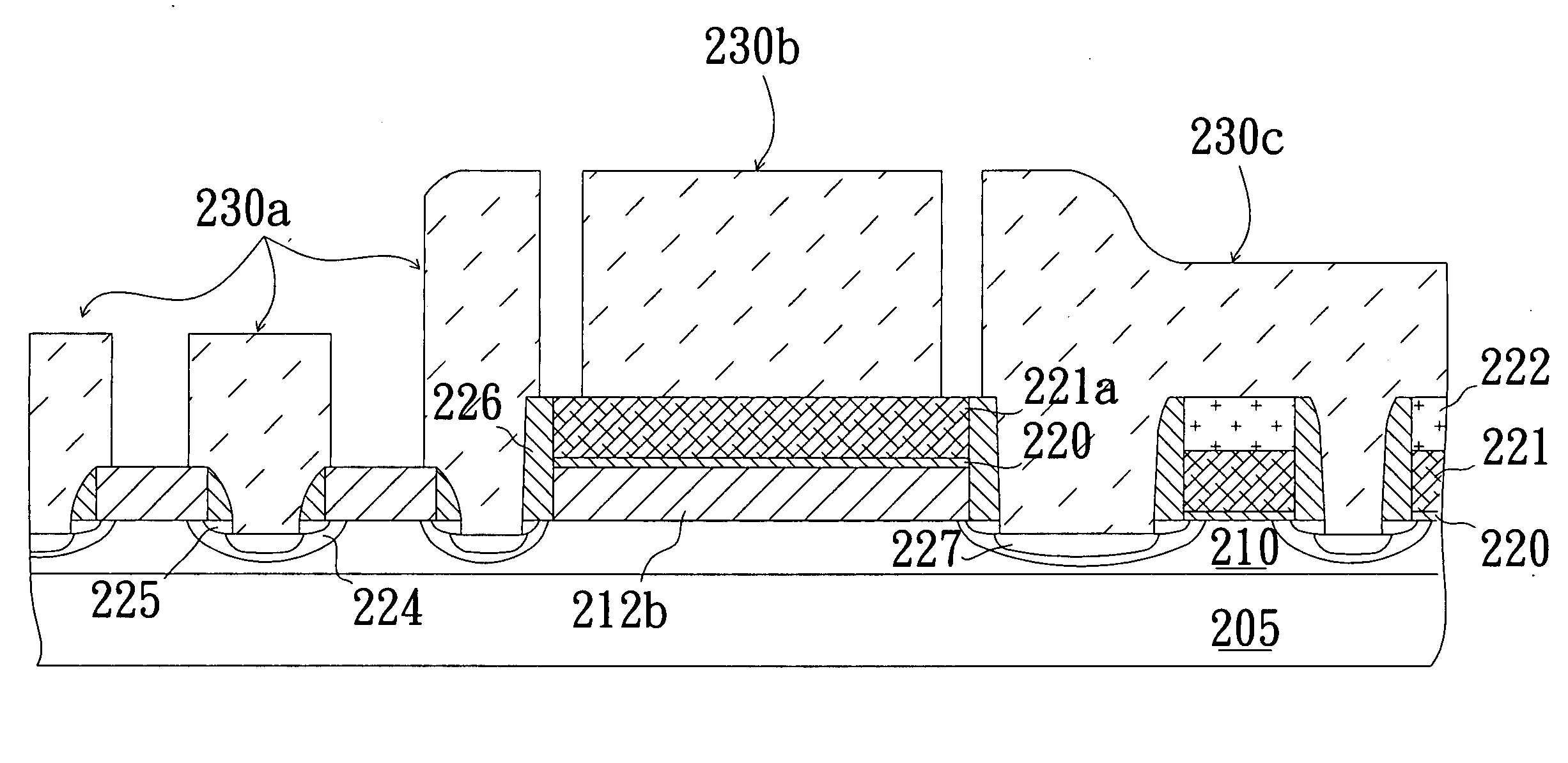
[0017]The main feature of the present invention resides on the fabrication step of forming a non-conductive layer, such as a field oxide layer or an ordinary silicon oxide layer, in the semiconductor fabrication process, which forms a non-conductive auxiliary structure in a transmitting region for locating the transmitting circuit. There may be a gate bus line and / or a data line formed on the transmitting region for transmitting a control signal or a data signal electrically coupled to each of the operating units in an operating region (or transistor region) of an integrated circuit to have the operating units operated according to the control signal. The non-conductive auxiliary structure partitions a plurality of spaces therein. The conductive layer formed on the non-conductive auxiliary structure fills the spaces such that even the conductive layer on the non-conductive auxiliary structure is removed by etching, some conductive material still remains in the spaces. The remained c...


PUM


Abstract

A semiconductor fabrication process according to the present invention defines an auxiliary structure with a plurality of spaces with a predetermined line-width in the oxide layer to prevent the conductive material in the spaces from being removed by etching or defined an auxiliary structure to rise the conductive structure so as to have the conductive structure being exposed by chemical mechanical polishing. Thus, the transmitting circuit can be defined without requiring an additional mask. Hence, the semiconductor fabrication process can reduce the number of required masks to lower the cost.

Description

FIELD OF THE INVENTION[0001]The present invention relates to a semiconductor structure and a fabrication method thereof, and more particularly to a double-diffused metal oxide semiconductor (DMOS) structure having a guard ring and a fabrication method thereof.BACKGROUND OF THE INVENTION[0002]As the function of present integrated circuits becomes more powerful and the structure of the integrated circuits becomes more complicated, the number of masks needed for fabricating the integrated circuits increases accordingly, and thus incurs a higher fabrication cost.[0003]With reference to FIGS. 1A to 1I for a fabrication process of an N-type double-diffused metal oxide semiconductor (DMOS) structure, an N-epitaxial layer 10 and a field oxide layer 12 are grown sequentially on a silicon substrate 5 as shown in FIG. 1A, and a first mask is used for forming a first photoresist layer 14 to define a region for locating a guard ring. In FIG. 1B, the exposed field oxide layer 12 is removed by etc...

Claims


Application Information

Patent Timeline
IPC IPC(8): H01L29/78H01L29/06H01L21/336
CPCH01L27/088H01L29/0619H01L29/7811H01L29/66719H01L29/66727H01L29/42372
Inventor TU, KAO-WAYTUNG, CHENG-HUI
Owner NIKO SEMICON
Why Eureka
Try Eureka