Organic light-emitting display apparatus and method of manufacturing the same

Active Publication Date: 2014-11-20
SAMSUNG DISPLAY CO LTD
View PDF11 Cites 2 Cited by
  • Summary
  • Abstract
  • Description
  • Claims
  • Application Information

AI Technical Summary

Benefits of technology

[0006]The present invention provides an organic light-emitting display apparatus having low resistance wiring

Problems solved by technology

When the active layer is formed of amorphous silicon, the mobility decreases such that it is difficult to produce a driving circuit that operates at high speeds.
When the active layer is formed of polysilicon, the mobility increases but a threshold voltage is not uniform such that it is necessary to arrange a separate compensation circuit.
Co

Method used


Image

  • Organic light-emitting display apparatus and method of manufacturing the same
  • Organic light-emitting display apparatus and method of manufacturing the same
  • Organic light-emitting display apparatus and method of manufacturing the same

Examples


Example

[0035]Hereinafter, the present invention will be described in detail by explaining exemplary embodiments of the invention with reference to the attached drawings. The invention may, however, be embodied in many different forms and should not be construed as being limited to the embodiments set forth herein; rather, these embodiments are provided so that this disclosure will be thorough and complete, and will fully convey the concept of the invention to those of ordinary skill in the art. Like reference numerals in the drawings may denote like or similar elements throughout the specification.

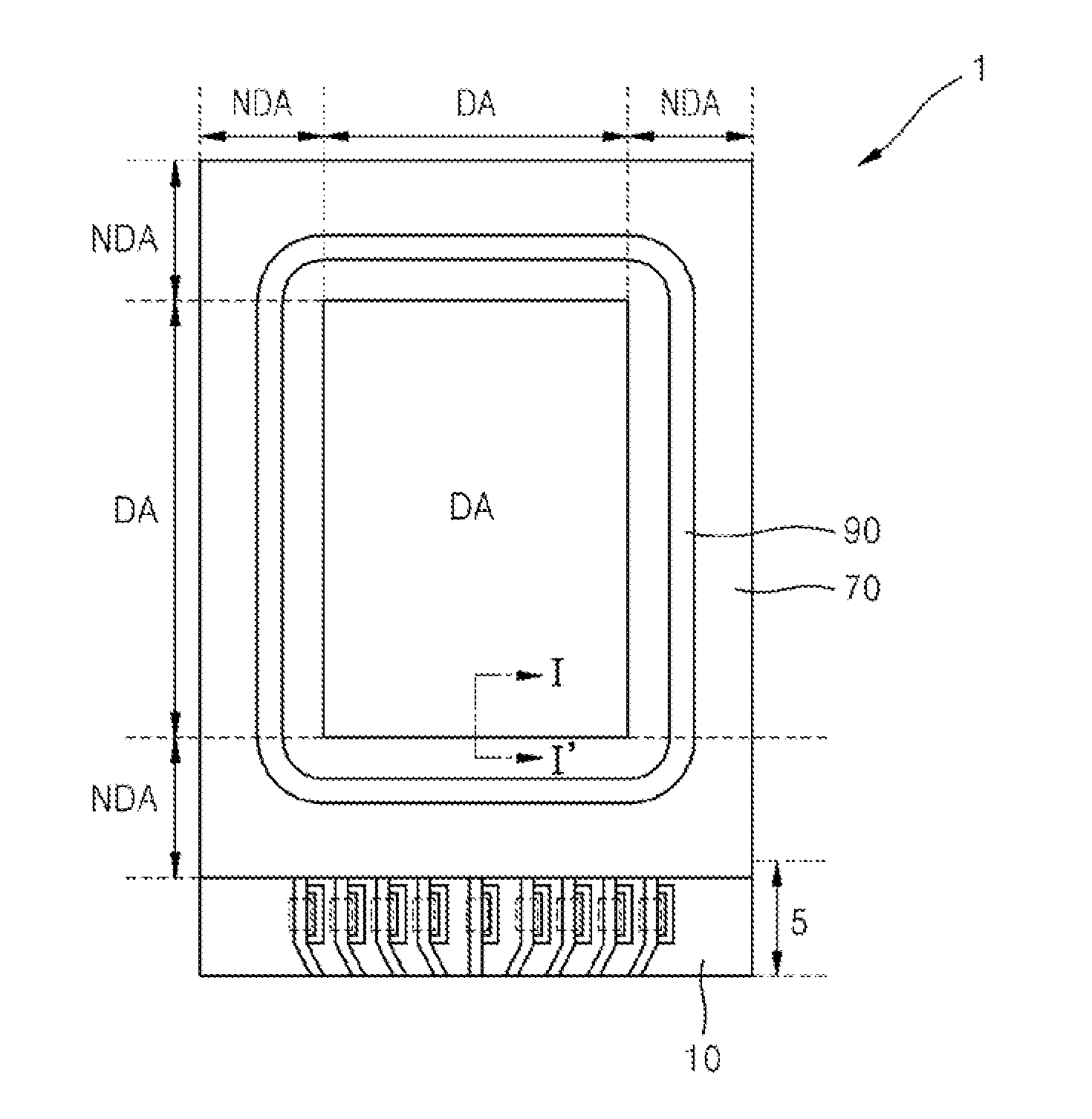
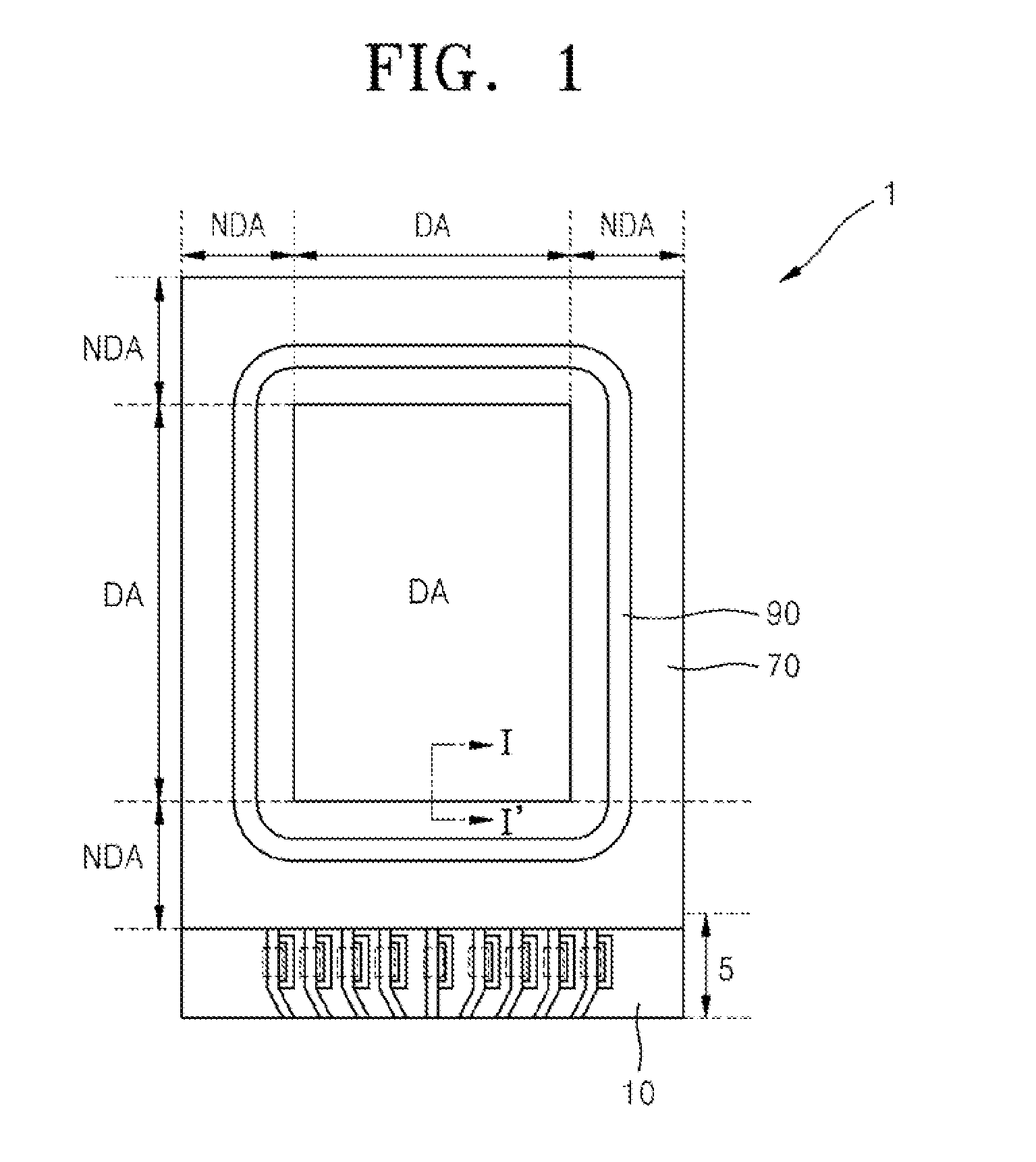
[0036]FIG. 1 is a plane view illustrating a structure of an organic light-emitting display apparatus 1 according to an embodiment of the present invention.

[0037]Referring to FIG. 1, the organic light-emitting display apparatus 1 includes a first substrate 10 and a second substrate 70, wherein the first substrate 10 includes a plurality of emission pixels and the second substrate 70 is bonded to t...


PUM


Abstract

An organic light-emitting display apparatus includes a substrate. A capacitor is formed on the substrate. The capacitor includes a first lower electrode, a second lower electrode, an upper electrode, a first insulating layer disposed between the first lower electrode and the second lower electrode, and a second insulting layer disposed between the second lower electrode and the upper electrode. A thin film transistor (TFT) includes a gate electrode disposed on a same layer as the first lower electrode, an active layer, and source and drain electrodes disposed on a same layer as the upper electrode. A wiring includes the same material layer as the second lower electrode.

Description

CROSS-REFERENCE TO RELATED PATENT APPLICATION[0001]This application claims priority to Korean Patent Application No. 10-2013-0055279, filed on May 15, 2013, in the Korean Intellectual Property Office, the disclosure of which is herein incorporated by reference in its entirety.TECHNICAL FIELD[0002]The present invention relates to a display apparatus, and more particularly, to an organic light-emitting display apparatus and a method of manufacturing the organic light-emitting display apparatus.DISCUSSION OF THE RELATED ART[0003]Flat panel display devices such as organic light-emitting display devices, liquid crystal display (LCD) devices, and the like are generally manufactured on a substrate on which a pattern, including a thin film transistor (TFT), a capacitor, and wiring for connecting the TFT and the capacitor, is formed. The TFT includes a gate electrode and an active layer. The active layer includes a channel region, a source region, and a drain region. The gate electrode is fo...

Claims


Application Information

Patent Timeline
IPC IPC(8): H01L27/32H01G4/30
CPCH01G4/30H01L27/3248H01L27/1255H10K59/123H10K59/1216H01L29/7869H05B33/10H10K59/124H10K59/1213
Inventor MO, YEON-GONKIM, MIN-KYU
Owner SAMSUNG DISPLAY CO LTD
Why Eureka
Try Eureka