Method of manufacturing semiconductor device, substrate processing apparatus and non-transitory computer-readable recording medium

Active Publication Date: 2015-10-08
KOKUSA ELECTRIC CO LTD
View PDF0 Cites 11 Cited by
  • Summary
  • Abstract
  • Description
  • Claims
  • Application Information

AI Technical Summary

Benefits of technology

[0008]However, the BCN film or the BN film formed by the technique may have a low oxidation resistance. Also, although such techniques are capable of decreasing a dielectric constant of the film to

Problems solved by technology

However, the BCN film or the BN film formed by the technique may have a low oxidation resistance.
Also, although such techniques are

Method used


Image

  • Method of manufacturing semiconductor device, substrate processing apparatus and non-transitory computer-readable recording medium
  • Method of manufacturing semiconductor device, substrate processing apparatus and non-transitory computer-readable recording medium
  • Method of manufacturing semiconductor device, substrate processing apparatus and non-transitory computer-readable recording medium

Examples


Example

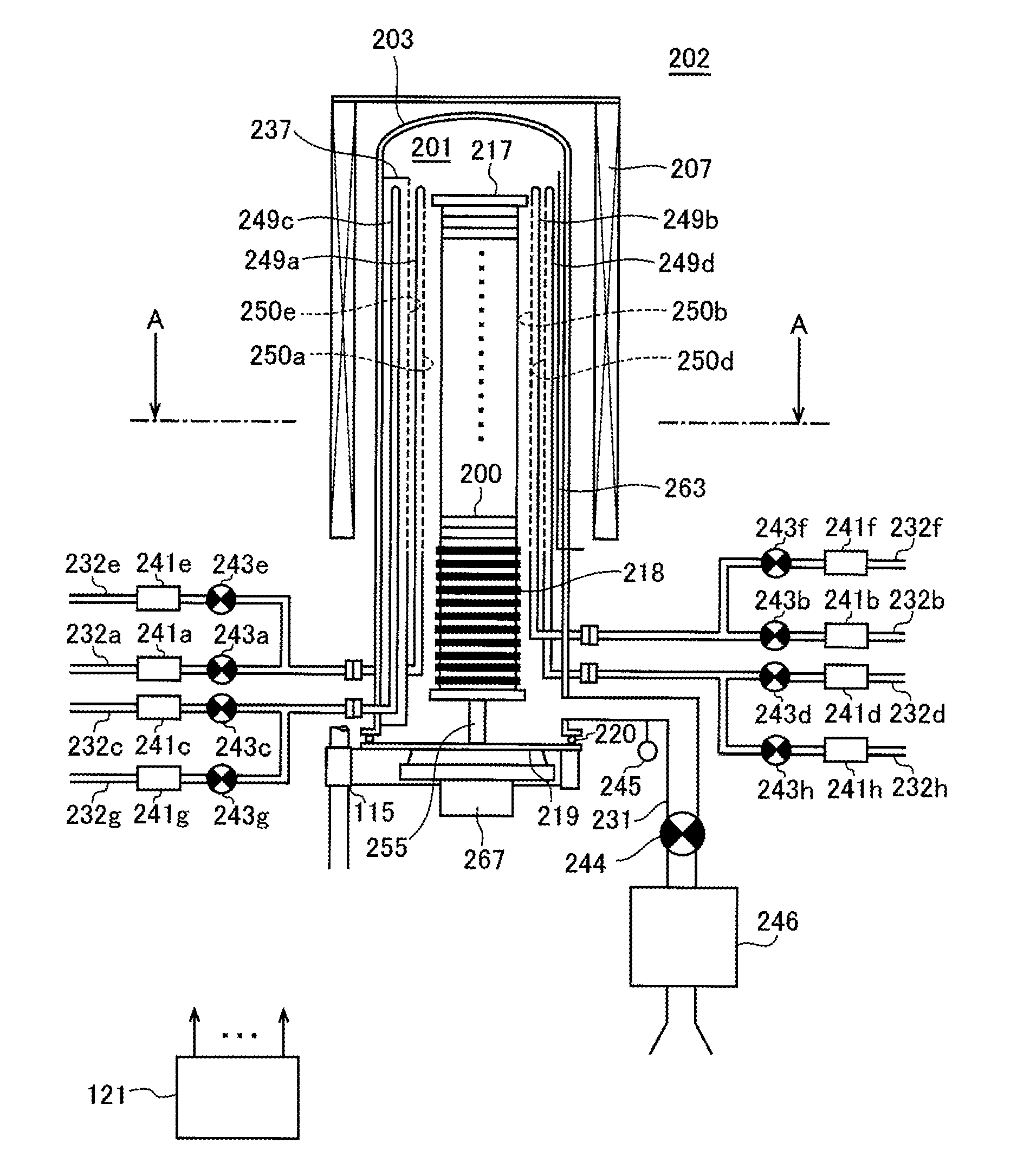
[0021]Hereinafter, the first embodiment of the present invention will be described with reference to FIGS. 1 and 3.

[0022](1) Configuration of Substrate Processing Apparatus

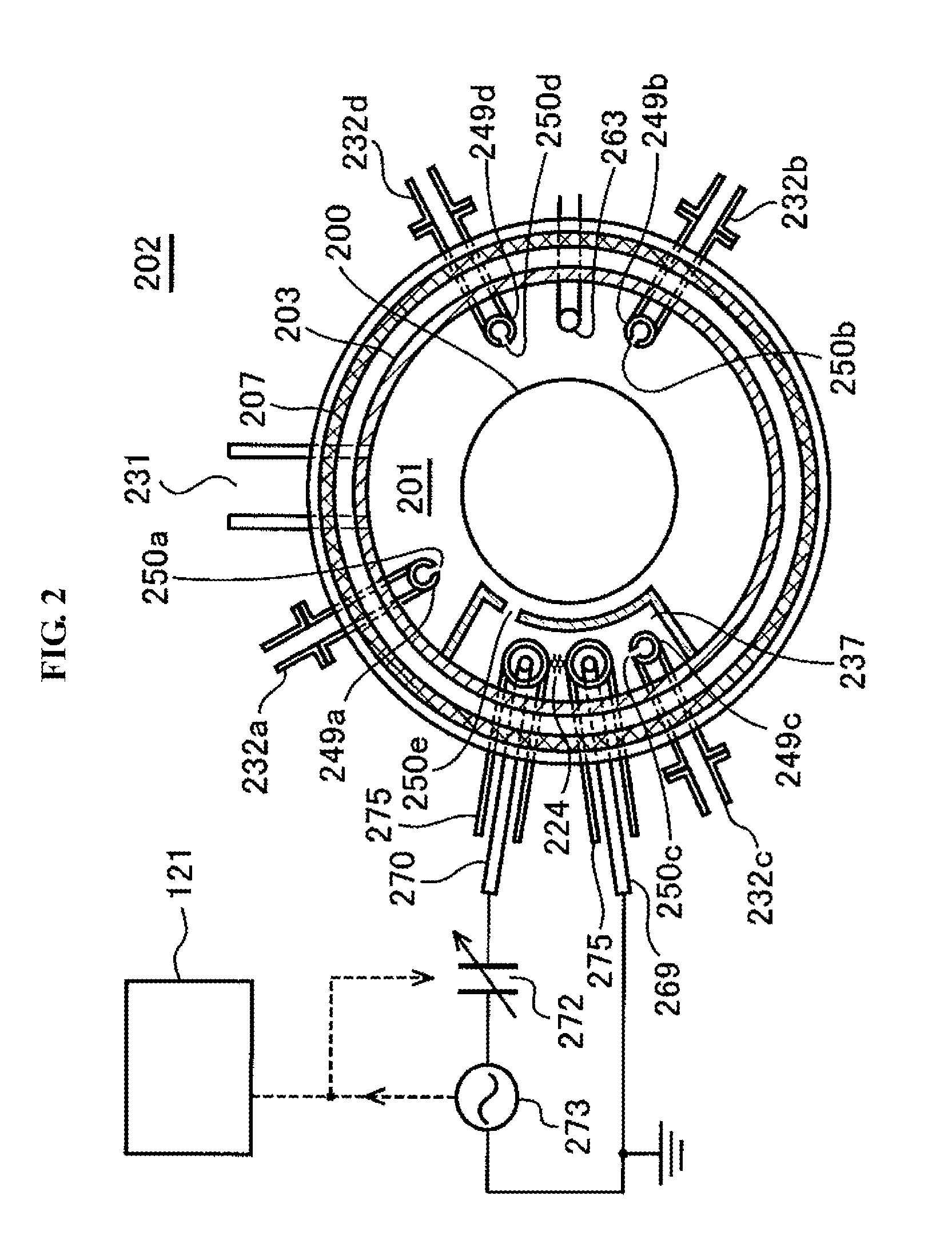
[0023]As illustrated in FIG. 1, a processing furnace 202 includes a heater 207 serving as a heating unit (heating mechanism). The heater 207 has a cylindrical shape and is vertically provided with support from a heater base (not illustrated) serving as a holding plate. As will be described below, the heater 207 also serves as an activating device (exciting unit) for activating (exciting) a gas by heat.

[0024]In the heater 207, a reaction tube 203 forming a reaction container (process container) is concentrically provided with respect to the heater 207. The reaction tube 203 is made of a heat-resistant material such as quartz (SiO2) or silicon carbide (SiC), and is formed in a cylindrical shape whose upper end is closed and lower end is opened. A process chamber 201 is formed in a cylindrical hollow portion of the r...

Example

Second Embodiment of the Present Invention

[0192]Next, the second embodiment will be described with reference to FIGS. 5A and 5B.

[0193]The first embodiment has exemplified the case in which the first set including steps S1a and S2a is performed a predetermined number of times to form the non-borazine-based BCN film on the wafer 200 in the process of forming the first film, the second set including steps S3a and S4a is performed a predetermined number of times to form the borazine-based BCN film on the non-borazine-based BCN film in the process of forming the second film, and the cycle including the process of forming the first film and the process of forming the second film is performed a predetermined number of times to form the laminate film. The present embodiment has a different process of forming the second film from the first embodiment. In the process of forming the second film of the present embodiment, a second set in which step S5b of supplying the nitriding gas to the wafe...

Example

Third Embodiment of the Present Invention

[0221]Next, the third embodiment will be described with reference to FIG. 6.

[0222]The present embodiment has a different process of forming the second film from the first embodiment. In the process of forming the second film of the present embodiment, a second set in which step S5c of supplying the amine-based gas to the wafer 200 is further included in addition to steps S3c and S4c that are the same as steps S3a and S4a is performed a predetermined number of times to form the borazine-based BCN film having a predetermined composition and a predetermined film thickness.

[0223]In the present embodiment, a laminate film in which the non-borazine-based BCN film and the borazine-based BCN film are laminated is formed on the wafer 200 by performing a cycle a predetermined number of times under a condition in which the borazine ring structure of the organic borazine-based gas (TMB gas) serving as the fourth process gas is preserved. The cycle includ...


PUM

PropertyMeasurementUnit
Thicknessaaaaaaaaaa
Thicknessaaaaaaaaaa
Structureaaaaaaaaaa

Abstract

Provided a method including forming a laminated film where a first film and a second film are laminated on a substrate by performing a cycle a predetermined number of times under a condition where a borazine ring structure in a fourth process gas is maintained. The cycle includes: (a) forming the first film by performing a first set a predetermined number of times, wherein the first set includes supplying a first process gas and supplying a second process gas to the substrate; and (b) forming the second film by performing a second set a predetermined number of times, wherein the second set includes supplying a third process gas and supplying the fourth process gas to the substrate.

Description

CROSS-REFERENCE TO RELATED PATENT APPLICATION[0001]This non-provisional U.S. patent application claims priority under 35 U.S.C. §119 of Japanese Patent Application No. 2014-076093, filed on Apr. 2, 2014, the entire contents of which are hereby incorporated by reference.BACKGROUND OF THE INVENTION[0002]1. Field of the Invention[0003]The present invention relates to a method of manufacturing a semiconductor device that includes a process of forming a thin film on a substrate, a substrate processing apparatus and a non-transitory computer-readable recording medium.[0004]2. Description of the Related Art[0005]Among processes of manufacturing a semiconductor apparatus (semiconductor device), a process of forming a boron nitride film (BN film) on a substrate such as a silicon wafer may be performed. Also, it is known that a hydrogen fluoride (HF) resistance of a film may increase when carbon (C) is contained in the BN film.RELATED ART DOCUMENTPatent Document[0006]1. Japanese Laid-open Pat...

Claims


Application Information

Patent Timeline
IPC IPC(8): H01L21/02C23C16/46C23C16/52C23C16/455
CPCH01L21/022H01L21/0228H01L21/02112C23C16/52C23C16/46C23C16/45557C23C16/45544C23C16/36C23C16/45529C23C16/45542C23C16/45546H01L21/67109
Inventor SANO, ATSUSHIHIROSE, YOSHIRO
Owner KOKUSA ELECTRIC CO LTD
Why Eureka
Try Eureka