Semiconductor device

Inactive Publication Date: 2013-10-31
HITACHI POWER SEMICON DEVICE
View PDF7 Cites 12 Cited by
  • Summary
  • Abstract
  • Description
  • Claims
  • Application Information

AI Technical Summary

Benefits of technology

[0009]Since the semiconductor device of the present invention has a novel termination structure, the withstand voltage of the semiconductor device can be designed to be higher than the withstand voltage determined by the concentration of the n−-type drift layer. Therefore, it is possible to provide a device with a low resistance while ensuring a withstand voltage. Alternatively, by decreasing the resistance of the device, it is possible to provide a device with low power loss.
[0010]FIG. 1 is an explanatory diagram showing a sectional structure of a termination part of a semiconductor device of a first embodiment of the present inv

Problems solved by technology

However, since the slope of the electric field in the substrate becomes steeper as the impurity concentration of t

Method used


Image

  • Semiconductor device
  • Semiconductor device
  • Semiconductor device

Examples


Example

First Embodiment

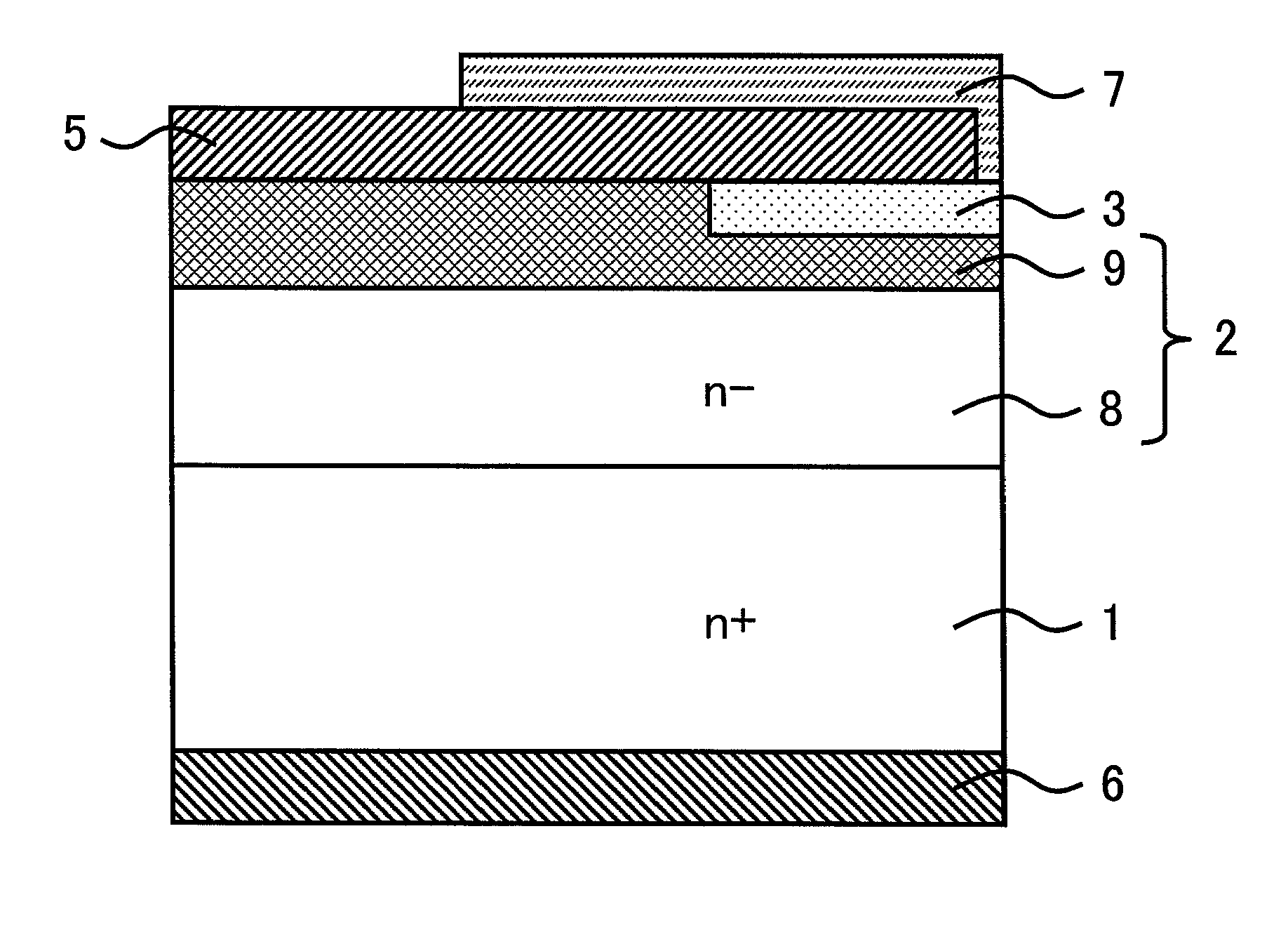
[0028]FIG. 1 is an explanatory diagram showing a sectional structure of a termination part of a semiconductor device of a first embodiment of the present invention. The semiconductor device according to the first embodiment is a diode including a low impurity concentration (n−-type) SiC drift layer 2 of a first conductivity type (n type) (hereinafter, referred to as “n−-type SiC drift layer 2”) formed on a high impurity concentration (n+-type) SiC substrate 1 of the first conductivity type (hereinafter, referred to as “n+-type SiC substrate 1”), a p-type semiconductor region 3 of a second conductivity type (p type) opposite to the first conductivity type, a p-type termination region (p-type semiconductor region) 4 of the second conductivity type (p type), an anode electrode 5 provided on a part of a front surface of the n−-type SiC drift layer 2, a cathode electrode 6 provided on a back surface of the n+-type SiC substrate 1, and an insulating film 7 provided on a pa...

Example

Second Embodiment

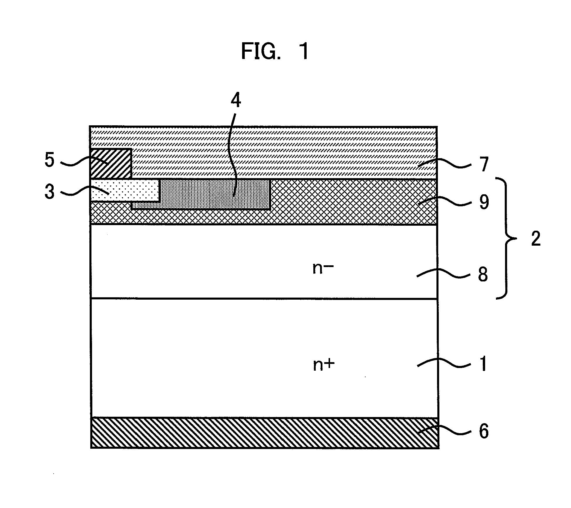
[0056]The n+-type SiC substrate 1 having the n−-type second semiconductor layer 9 formed on the entire upper surface of the n−-type SiC drift layer 2 is used in the first embodiment, but the n−-type second semiconductor layer 9 may be formed in a part of the region on the upper surface of the n−-type SiC drift layer 2 so as to cover a pn junction formed in a lateral direction. This is because the device withstand voltage at the time of applying a reverse voltage depends on the structure of the active region and the termination structure and the device withstand voltage can be improved also by the increase of the withstand voltage by the termination structure. FIG. 14 and FIG. 15 show the sectional structures in this case. In the case of these structures, in addition to the effects of the first embodiment, there is an advantage that the termination structure can be designed separately from and independently of device design.

[0057]FIG. 14 shows an example in which the...

Example

Third Embodiment

[0060]FIG. 16 is an explanatory diagram showing a sectional structure of a semiconductor device of a third embodiment of the present invention. The third embodiment provides an example in which a so-called trench-gate junction field-effect transistor (JFET) is formed in an active region. For avoiding complications, the gate electrode, the source electrode, and the insulating film 7 for protecting the front surface are omitted. The semiconductor device of the third embodiment is different from a general trench-gate JFET in that a stacked film formed of the n−-type first semiconductor layer 8 and the n−-type second semiconductor layer 9 whose impurity concentration is higher than that of the n−-type first semiconductor layer 8 is used as the n−-type SiC drift layer 2 and the pn junction of a gate and the JTE where the electric field may possibly concentrate are formed in the n−-type second semiconductor layer 9. The manufacturing method and structure other than that ma...


PUM


Abstract

On a front surface of a region where a junction termination extension structure of a semiconductor device using silicon carbide is formed, a structure having an n-type semiconductor region with a concentration relatively higher than a concentration of an n-type drift layer is formed. An edge of the junction termination extension structure located on a side away from an active region is surrounded from its bottom surface to its front surface by an n-type semiconductor region. By this means, it is possible to provide a device with a low resistance while ensuring a withstand voltage, or by decreasing the resistance of the device, it is possible to provide a device with low power loss.

Description

TECHNICAL FIELD[0001]The present invention relates to a semiconductor device, and in particular to a technology effectively applied to a termination structure of a semiconductor device using silicon carbide.BACKGROUND ART[0002]Silicon carbide semiconductor (SiC) has features of a larger bandgap and a higher dielectric breakdown field intensity approximately by one order of magnitude compared with silicon semiconductor, and therefore is viewed as a promising material for a power device. In particular, when a unipolar device operating only with majority carriers is used, this is effective for the reduction of loss at the time of switching operation because there is no reverse current generated at the time of switching operation in a bipolar device (process of disappearance of excessive minority carriers).[0003]On the other hand, when a unipolar device is used, the resistance at the time of forward operation and the withstand voltage at the time of applying a reverse voltage are determ...

Claims


Application Information

Patent Timeline
IPC IPC(8): H01L29/16
CPCH01L29/1608H01L29/0615H01L29/0692H01L29/0843H01L29/0878H01L29/1095H01L29/6606H01L29/7811H01L29/8083H01L29/861H01L29/872H01L29/80H01L29/808H01L29/47H01L29/78H01L29/06H01L29/12
Inventor KAMESHIRO, NORIFUMISHIMIZU, HARUKA
Owner HITACHI POWER SEMICON DEVICE
Why Eureka
Try Eureka