

TFT array substrate and method for producing the same
- Summary
- Abstract
- Description
- Claims
- Application Information
AI Technical Summary
Benefits of technology
Problems solved by technology
Method used
Image

Examples
first preferred embodiment
[0032]The present invention relates to a FFS mode liquid crystal display device in which liquid crystal is held between a TFT array substrate and an opposed substrate, and the TFT array substrate has a characteristic structure. This preferred embodiment shows a case where the present invention is applied to a TFT array substrate provided with an inversely-staggered TFT.
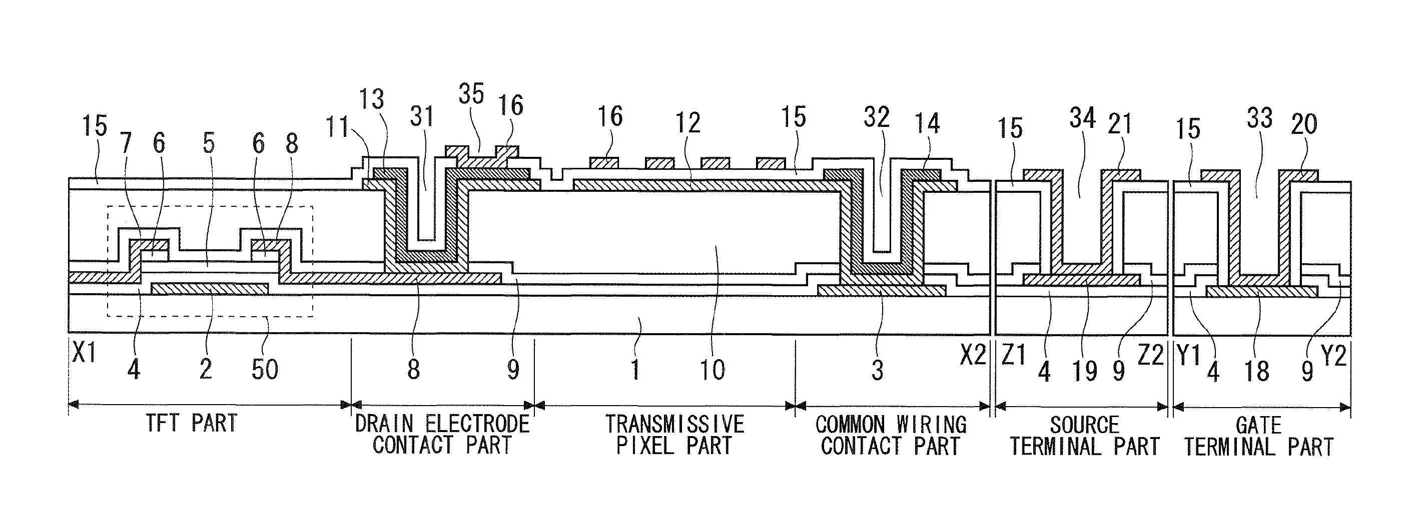
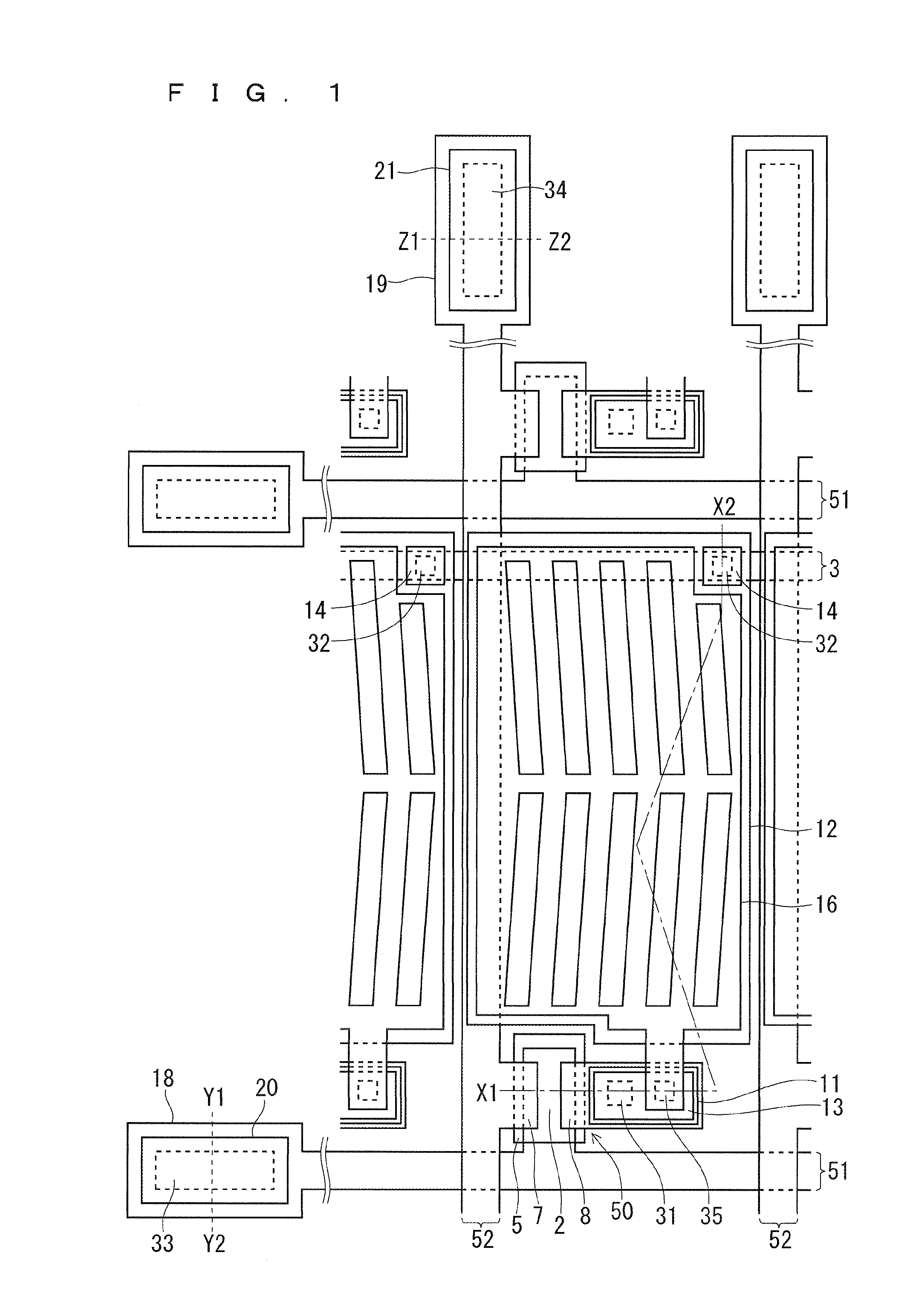
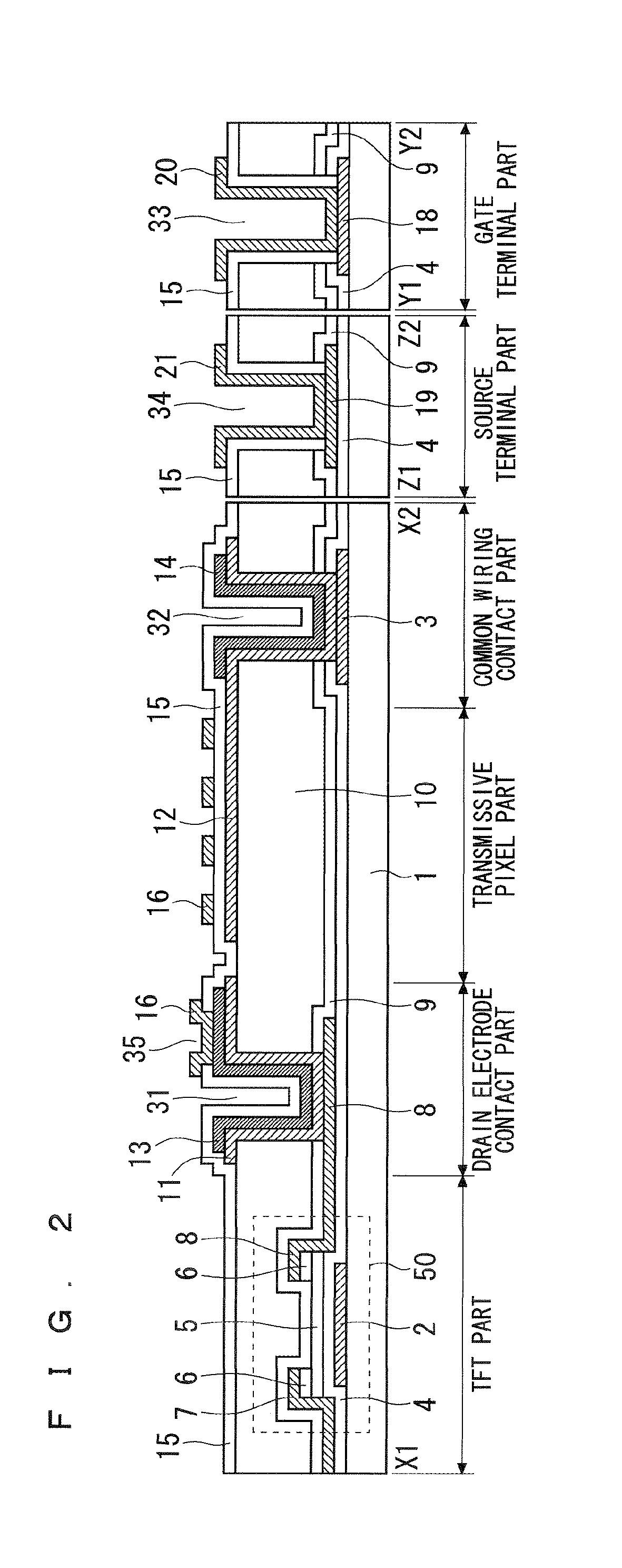
[0033]FIG. 1 is a plan view showing a configuration of a TFT array substrate according to a first preferred embodiment. In addition, FIG. 2 shows cross-sectional views of the TFT array substrate, corresponding to cross-sectional surfaces taken along lines X1-X2, Y1-Y2, and Z1-Z2 in FIG. 1.
[0034]In addition, in the cross-sectional surface taken along the line X1-X2 in FIG. 2, a “TFT part” shows a region where a TFT element 50 which will be described below is formed, a “drain electrode contact part” shows a region where a drain electrode contact hole 31 which will be described below is formed, a “transmissive pixel part...
second preferred embodiment
[0076]A large number of photoengraving steps (that is, the number of masks) is needed to form the FFS mode TFT array substrate including the organic insulating film serving as the planarizing insulating film, so that a producing time is long and production cost is high. Thus, this second preferred embodiment proposes a production method in which the required number of masks is reduced, and production process can be simplified.
[0077]A TFT array substrate in the second preferred embodiment includes a staggered type TFT element having a top gate structure. In this case, an amorphous silicon is used for a semiconductor layer, but polysilicon or microcrystalline silicon may be used therefor.
[0078]FIG. 6 is a plan view showing a configuration of the TFT array substrate according to the second preferred embodiment. In addition, FIG. 7 shows cross-sectional views of the TFT array substrate corresponding to cross-sectional surfaces taken along lines X1-X2, Y1-Y2, and Z1-Z2 in FIG. 6. In the ...
third preferred embodiment
[0098]A third preferred embodiment proposes a method for producing FFS mode TFT array substrate in which the number of masks is further reduced.
[0099]Like in the second preferred embodiment, in the case where the semiconductor layer 5 is formed of low-temperature polysilicon, amorphous silicon, microcrystalline silicon, or the like, a carrier is photoexcited by backlight because a bandgap of each material is small. As a result, an off leakage current is generated, and the problems such as crosstalk and display unevenness are generated when an image is displayed. According to the second preferred embodiment, in order to solve this problem, the light blocking film 24 is provided under the semiconductor layer 5.
[0100]However, in a case where an oxide semiconductor having a large bandgap is used for the semiconductor layer 5, such a problem is not generated, so that the light blocking film 24 is not needed, and the number of masks required in the production process can be reduced. Furth...
PUM
 Abstract
Description
Claims
Application Information