Low temperature carbon rich oxy-nitride for improved RIE selectivity

Inactive Publication Date: 2002-11-26
IBM CORP +1
View PDF9 Cites 25 Cited by
  • Summary
  • Abstract
  • Description
  • Claims
  • Application Information

AI Technical Summary

Problems solved by technology

One problem with the current SAC and nitride liner process is that it requires high temperatures (720-800.degree. C.).
Improvement in contact shorts yield is still one of the main issues facing many DRAM producing fabricators.
During etching processes, when this surface carbonization is broken through, undercutting during etch occurs rapidly.
However, the ar

Method used


Image

  • Low temperature carbon rich oxy-nitride for improved RIE selectivity
  • Low temperature carbon rich oxy-nitride for improved RIE selectivity
  • Low temperature carbon rich oxy-nitride for improved RIE selectivity

Examples


Embodiment Construction

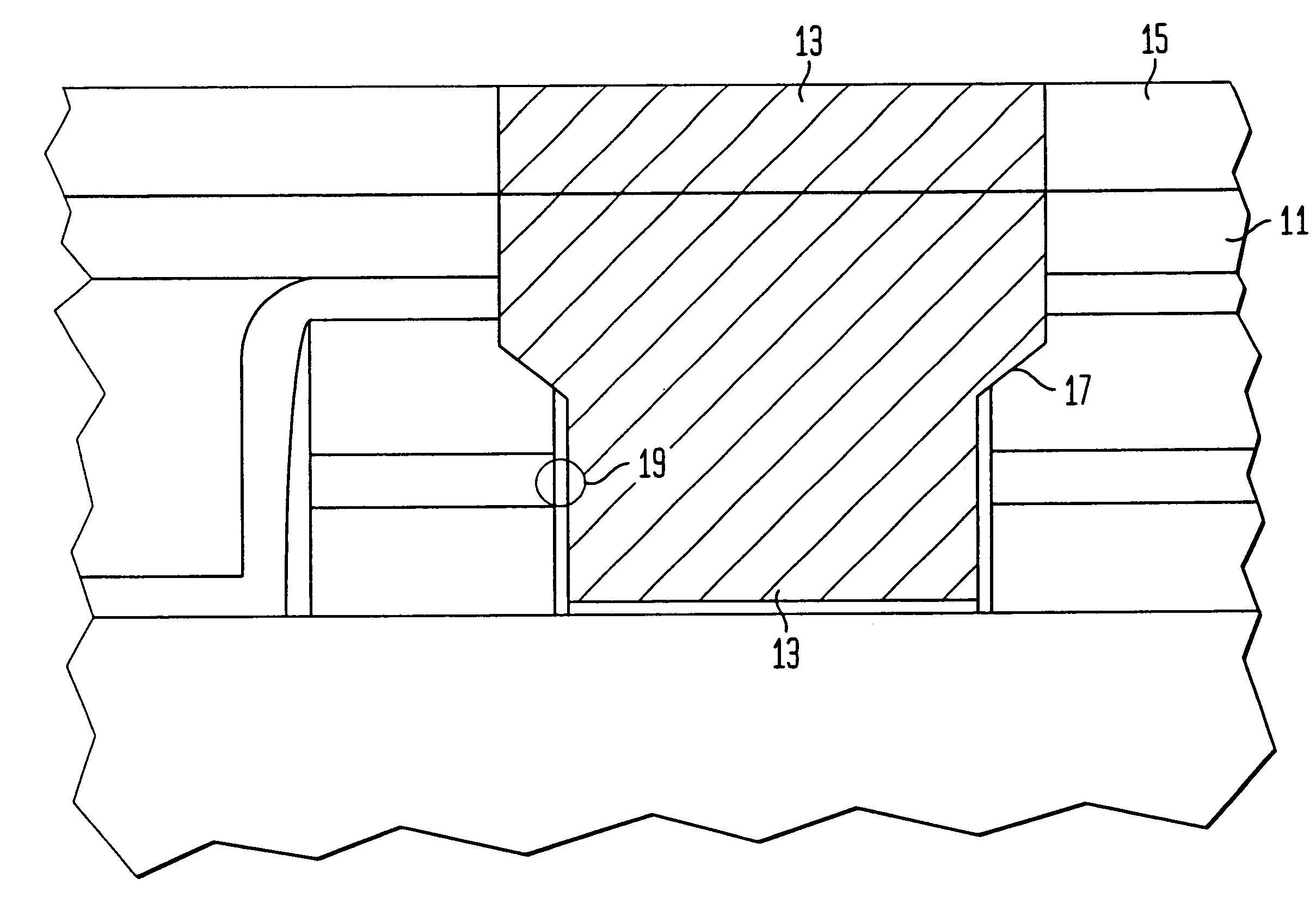
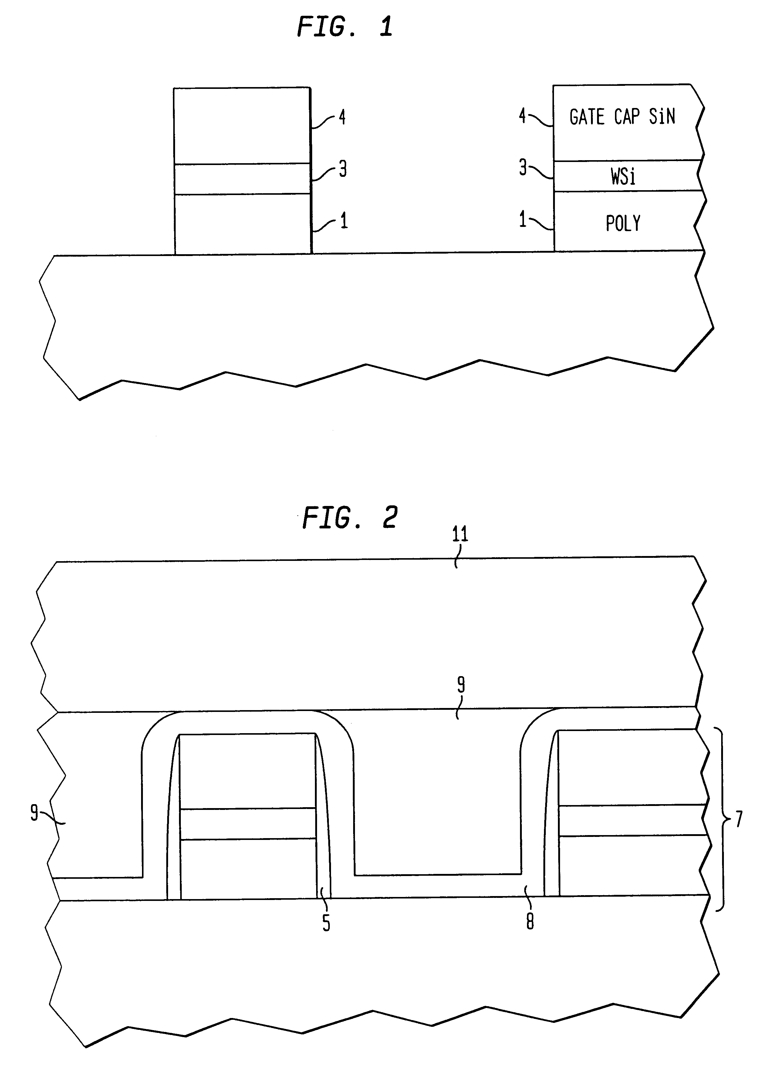
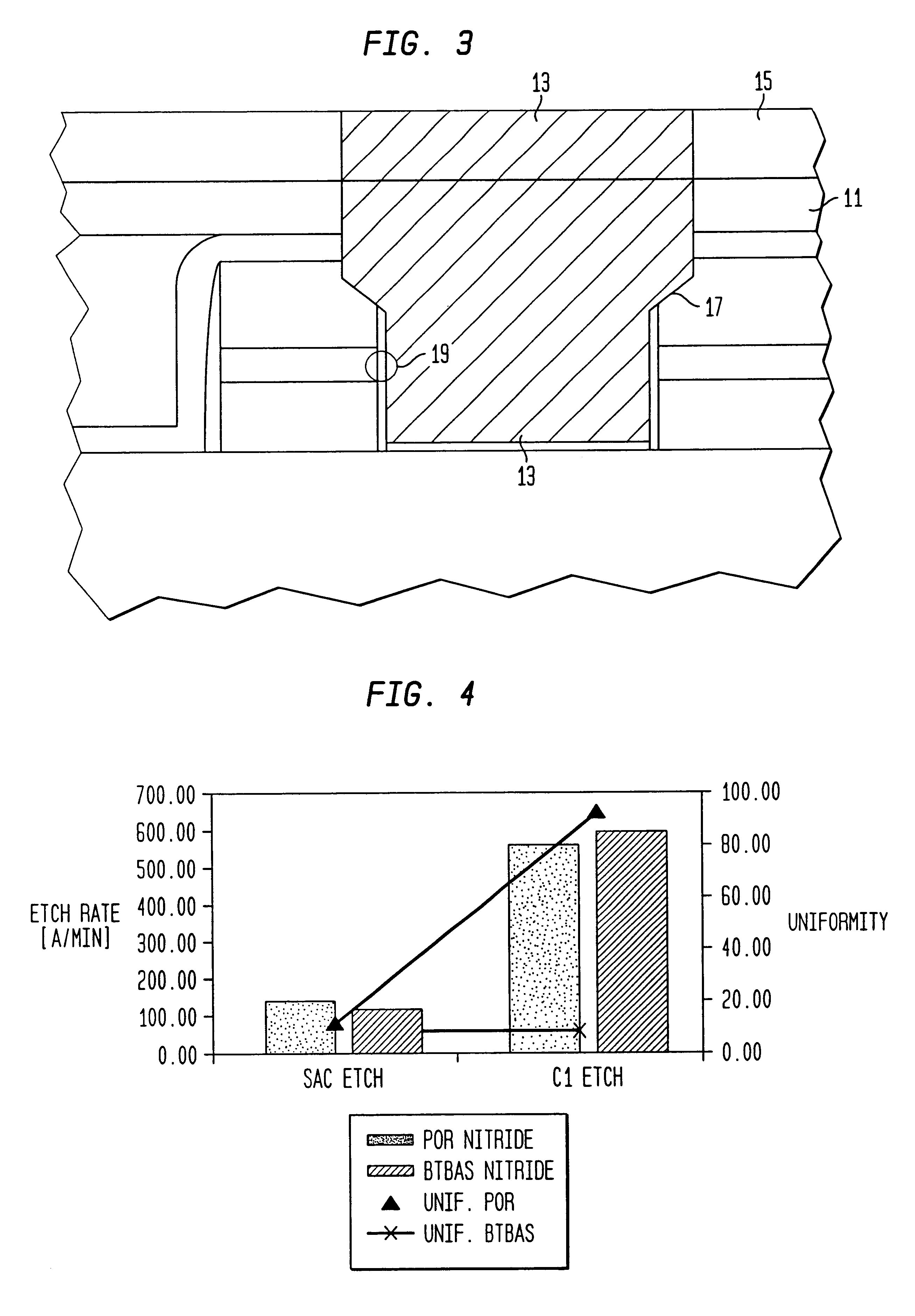
Referring now to the drawings, and more particularly to FIGS. 1-3, which illustrate three stages in the formation of a bit line contact. The first stage is shown in FIG. 1. As can be seen, gate stack deposition comprised of polysilicon layer 1, a tungsten suicide layer 3, and a gate cap silicon nitride 4 is deposited on a portion of a chip. The gate stack is etched to form gates.

FIG. 2 shows the cross section after deposition of spacer nitride, boro phospho silicate glass deposition, chemical mechanical polish, silicon dioxide deposition, and anneal. As can be seen, the spacer nitride 5 is deposited against each gate stack 7. A deposition of silicon oxy nitride 8 covers the exposed surface of the chip as well as the sides and top of the gate stack. Boro phospho silicate glass (BPSG) 9 fills in the depth between and over the gate stacks 7. A chemical mechanical polish smooths the surface of the BPSG 9, followed by a silicon dioxide 11 deposition and anneal.

Formation of carbon contain...


PUM


Abstract

Reactive ion etch (RIE) selectivity during etching of a feature nearby embedded structure is improved by using a silicon oxynitride layer formed with carbonization throughout layer.

Description

1. Field of the InventionThe present invention generally relates to DRAM fabrication and more particularly to self-aligned contact etching.2. Background DescriptionA self-aligned contact (SAC) etch is one of the most difficult reactive ion etch (RIE) processes in a DRAM fabrication sequence. It is a three step process utilizing different etch chemistries. Step one is a non-selective or traditional oxide etch of silicon dioxide to the gate cap Nitride. The next step involves the etching of borophosphorous silicate glass (BPSG) with a very high selectivity to Nitride liner and gate cap Nitride, which tests the limit of a RIE tool. Finally, in the third step the bottom liner is removed through to a silicon substrate so that an ohmic contact can be formed subsequently.One problem with the current SAC and nitride liner process is that it requires high temperatures (720-800.degree. C.). A reduced thermal budget is preferred in future generations of DRAM devices to minimize dopant diffusio...

Claims


Application Information

Patent Timeline
IPC IPC(8): H01L21/02H01L21/311H01L21/70H01L21/8242H01L21/316H01L21/314
CPCH01L21/02126H01L21/02222H01L21/02271H01L21/31116H01L21/76834H01L21/76897H01L27/10855H01L27/10888H10B12/485H10B12/0335
Inventor CHAUDHARY, NIRMALCONTI, RICHARD A.
Owner IBM CORP
Why Eureka
Try Eureka