
Structure and method for air cavity packaging

a technology of structure and method, applied in the direction of semiconductor devices, semiconductor/solid-state device details, electrical devices, etc., can solve the problems of reducing the performance of dies, reducing the frequency of devices, and voids in adhesive agents that occur frequently, so as to reduce the occurrence of voids and improve packaging quality and yield.

Inactive Publication Date: 2014-04-17
WIN SEMICON
View PDF0 Cites 19 Cited by
  • Summary
  • Abstract
  • Description
  • Claims
  • Application Information

AI Technical Summary

Benefits of technology

This patent aims to provide a structure for air cavity packaging with air vents that can exhaust air from the air cavities during the curing of adhesive agent. This reduces the occurrence of voids and improves the quality and yield of the packaged products. Additionally, multiple packages can be produced simultaneously.

Problems solved by technology

For high frequency devices, however, the conventional packaging method may suppress high frequency performance of the devices.
In the conventional air cavity packaging, however, while curing the adhesive agent by heating, voids occur frequently in the adhesive agent owing to the air in the air cavity exhausting to the outside.
If plural connected packages are produced at once, the adhesive agent will overflow to the adjacent packages due to the release of the air pressure from the air cavities, which leads to degradation of the performance of the dies.
Therefore, in the conventional air cavity packaging, usually only one package is produced at one time to prevent the problem of voids and adhesive agent overflow, which limits the yield of packages.

Method used


Image

  • Structure and method for air cavity packaging
  • Structure and method for air cavity packaging
  • Structure and method for air cavity packaging

Examples


Embodiment Construction

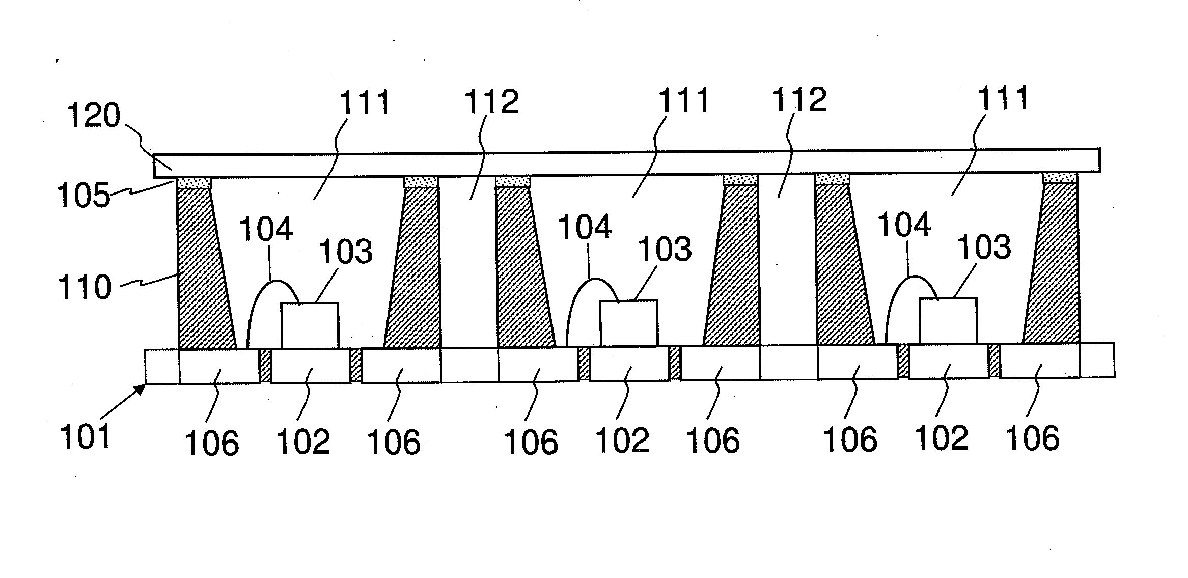
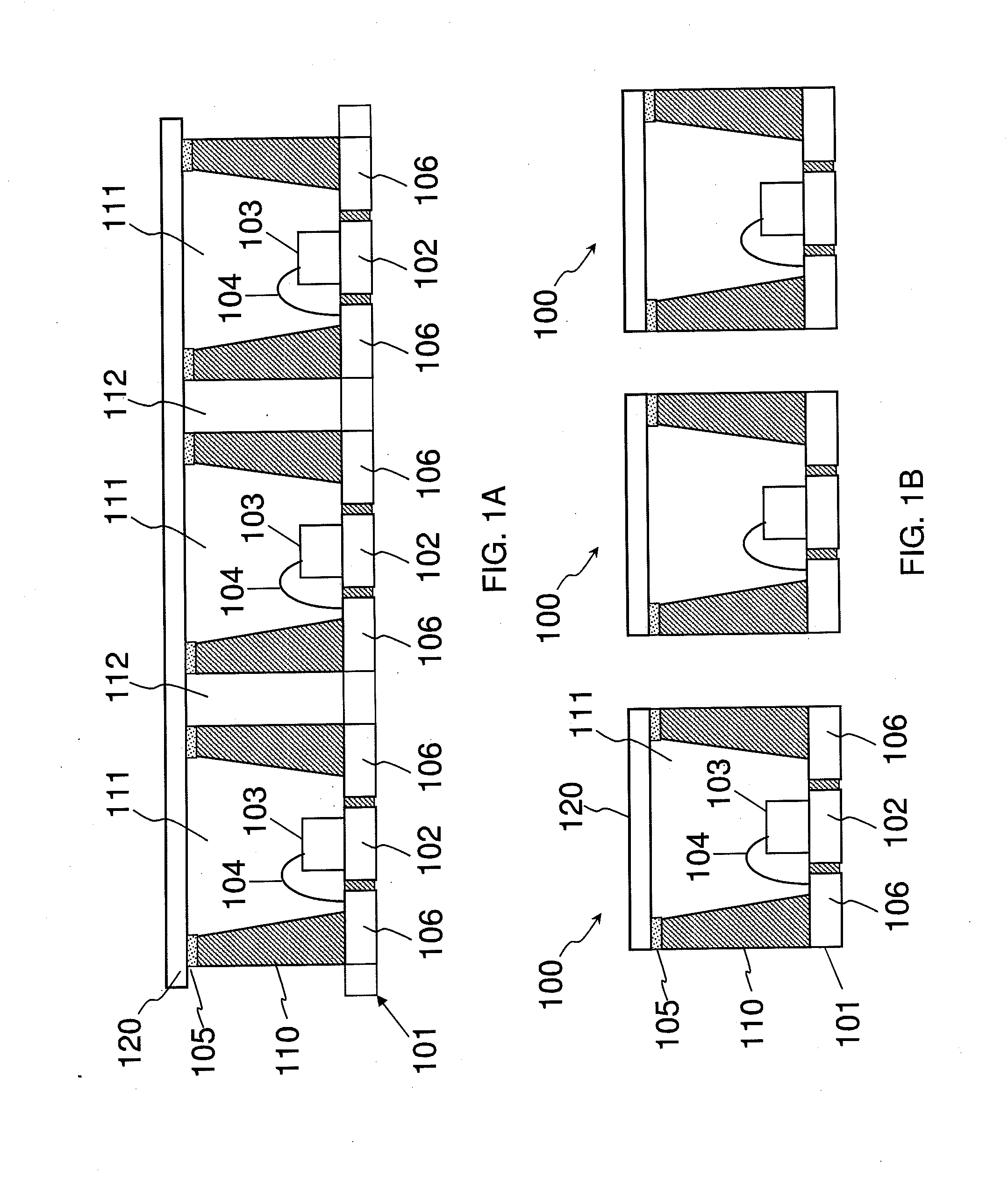
[0034]FIG. 1A is a schematic showing a cross-sectional view of an embodiment of a structure for air cavity packaging according to the present invention, which comprises a carrier 101, plural dies 103, plural wires 104, plural walls 110, and a lid 120. The carrier 101 comprises plural die pads 102 and plural leads 106. Each of the plural dies 103 is mounted on a die pad 102. The plural wires 104 electrically connect the plural dies 103 to the plural leads 106. The plural walls 110 are disposed on the carrier 101 and form plural cavities 111 in a way that each cavity 111 contains at least one die pad 102 and plural leads 106, and each wall 110 is provided with at least one air vent 112 for exhausting air to the outside. The lid 120 is attached on the plural walls 110 by means of an adhesive agent 105, so that the plural cavities 111 are sealed to plural sealed cavities. By dicing the package structure shown in FIG. 1A, plural air cavity packages 100 as shown in FIG. 1B can be produced...


PUM


Abstract

A structure and method for air cavity packaging, the structure comprises a carrier having plural die pads and leads, plural dies, plural wires, plural walls, and a lid. The dies are mounted on the die pads. The wires electrically connect the dies to the leads. The plural walls are disposed on the carrier and form plural cavities in a way that each cavity contains at least one die pad and plural leads, and each wall is provided with at least one air vent for exhausting air to the outside. The lid is attached on the plural walls via an adhesive agent to seal the plural air cavities, so that the plural connected air cavity packages are formed.

Description

FIELD OF THE INVENTION[0001]The present invention relates to a structure and method for semiconductor dies packaging, and more particularly, to a structure and method for air cavity packaging used for high frequency or high power semiconductor devices.BACKGROUND OF THE INVENTION[0002]After the fabrication of semiconductor dies, a packaging process is required to provide the dies support and to protect them against the moisture corrosion or any other damage. A conventional semiconductor dies packaging process includes die bonding, then wire bonding, and finally used molding compound to seal the package, so that the circuits on the dies can be protected against the moisture corrosion. For high frequency devices, however, the conventional packaging method may suppress high frequency performance of the devices. In the air cavity packaging method, a sealed cavity is formed around the dies in the package. The medium in the package is gas (e.g., vacuum, nitrogen, air), which can provide go...

Claims


Application Information

Patent Timeline
Patent Type & Authority Applications(United States)
IPC IPC(8): H01L23/498H01L21/50
CPCH01L21/50H01L23/498H01L24/97H01L2224/48247H01L2224/97H01L23/047H01L23/10H01L23/495H01L23/49861H01L2924/1461H01L2924/181H01L2924/16195H01L2224/85H01L2924/00
Inventor FU, ZI-HONGYANG, SUNG-MAOCHU, CHUN-TINGHSU, WEN-CHING
Owner WIN SEMICON
Learn More