
Eureka
For R&D, Eureka makes reading and utilizing patents & technical documents easy.
Eureka AIR
Designed for self-driven R&D workflows. Generate viable solutions, solve complex R&D challenges, empower your innovation with AI.

Eureka Materials
Designed for material experts only. Revolutionize your material R&D, from search, analyze, to developing new materials.

TechResearch
Generate reliable direction feasibility study reports for your R&D in just a few steps.

TechSeek
Discover and master advanced knowledge NOW. Basics, ideas, possibilities, all at once.

TechMind
As an expert in R&D Theories, TechMind can generates customized viable solutions instantly.

TechRisk
Analyze your overall solution with one click, know your potential R&D risks in advance.

TechMonitor
Get weekly tech updates, stay abreast of the latest tech innovations and key insights.
Device and method for writing/reading a memory register shared by a plurality of peripherals
- Summary
- Abstract
- Description
- Claims
- Application Information
AI Technical Summary
Benefits of technology
Problems solved by technology
Method used
Image

Examples
Embodiment Construction
[0037]Although this is not expressly shown, the individual features described with reference to each embodiment shall be intended as auxiliary and / or interchangeable with other features, as described with reference to other embodiments.
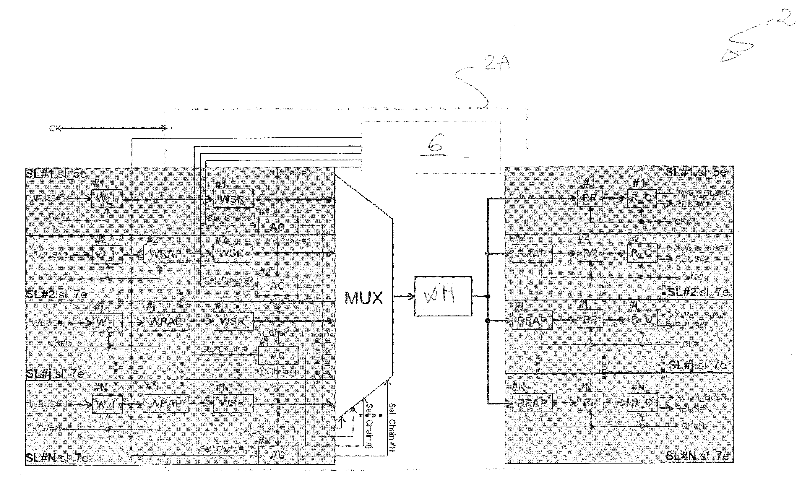
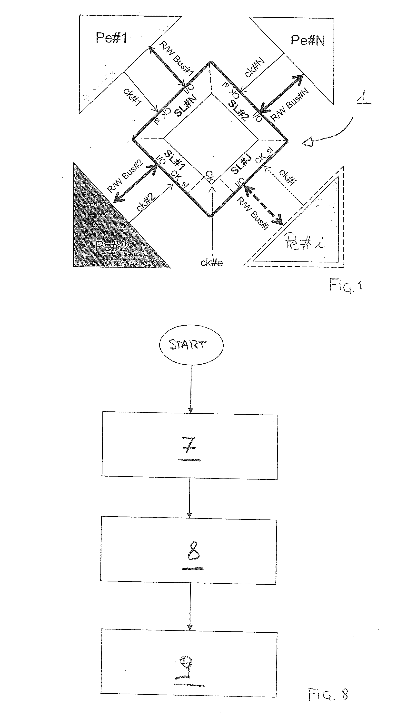
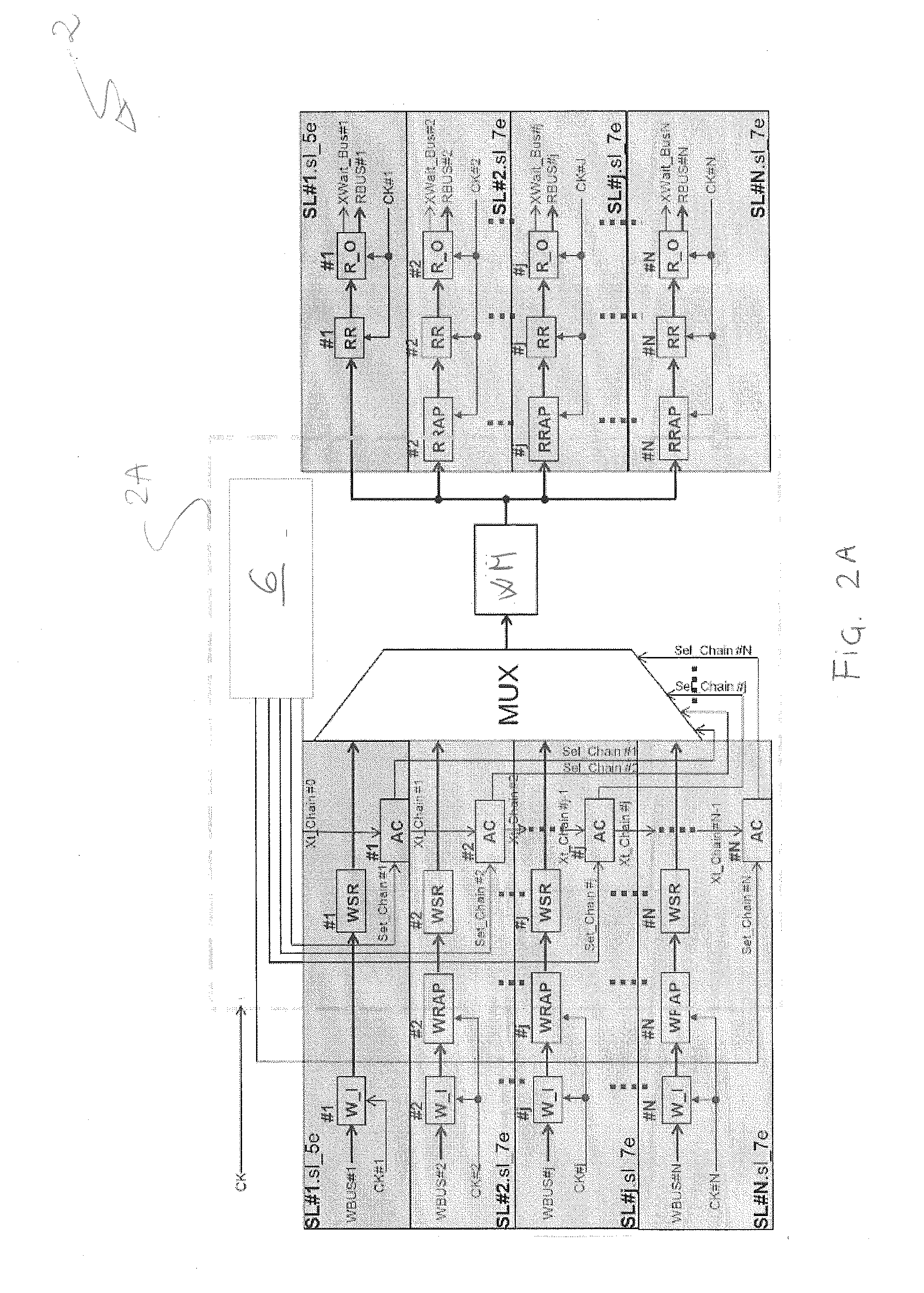
[0038]The present disclosure relates to a digital writing / reading device 1, which may be implemented in discrete form or integrated in a so-called “System On Chip” (SOC), having N peripherals Pe#1, . . . , Pe#N, each generally operating with its own clock signal ck#1, . . . , ck#N, which is asynchronous to an external clock signal ck#e and to the other N−1 peripheral clock signals.
[0039]Particularly, multiple peripherals may have the same clock signal, which may in turn be different from or equal to the external clock ck#e.
[0040]It shall be noted that the example of FIGS. 1 and 2A will be explained hereinbelow, in which the clock signal ck#1 is assumed to be equal to the external clock signal ck#e, to describe the operation of two types of modules, as...
PUM
 Abstract
Description
Claims
Application Information
 - R&D Engineer
- R&D Manager
- IP Professional
- Industry Leading Data Capabilities
- Powerful AI technology
- Patent DNA Extraction
Browse by: Latest US Patents, China's latest patents, Technical Efficacy Thesaurus, Application Domain, Technology Topic, Popular Technical Reports.
© 2024 PatSnap. All rights reserved.Legal|Privacy policy|Modern Slavery Act Transparency Statement|Sitemap|About US| Contact US: help@patsnap.com