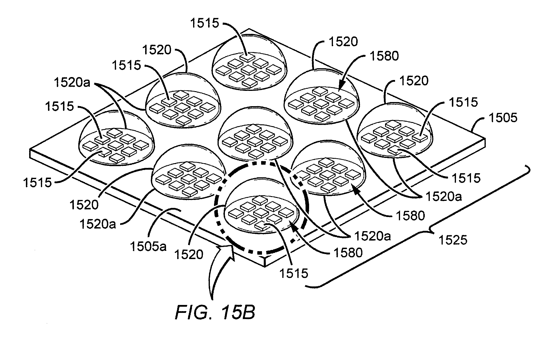
Tilted emission LED array
a technology of led arrays and led components, applied in the direction of basic electric elements, semiconductor devices, electrical equipment, etc., can solve the problems of difficult use of complex and expensive mounting configurations or hardware, special, expensive lens tooling and lens fabrication processes, and may not be advantageous for all. , to achieve the effect of improving light fixture emission and emission characteristics
- Summary
- Abstract
- Description
- Claims
- Application Information
AI Technical Summary
Benefits of technology
Problems solved by technology
Method used
Image

Examples
example 1
[0119]The change in the intensity distribution that results from purposely moving LED chips off-center with respect to an overlying lens is explored in this example. FIG. 13A is a photograph of an exemplary LED component including 12 LED chips, each with its own hemispherical lens. Three cases are examined: LED chip 1315 at lens 1320 optical center (center of lens base 1320a) (FIG. 13C); LED chip 1315 offset radially inward (FIG. 13D); and LED chip 1315 offset radially outward (FIG. 13E). The chip 1315 physical offset is ˜220-230 micrometers in a 3.0 mm diameter lens 1320.
[0120]The chart in FIG. 13B shows that the amount of light as a function of angle from the perpendicular is different for offset chip placement vs. an on-axis placement case. In particular, offsetting the LED chip 1315 as described with respect to the overlying lens 1320 leads to a broadening of the intensity beam profile. For this example, the difference in light output varies by angle and is maximum in the 30-60 ...
example 2
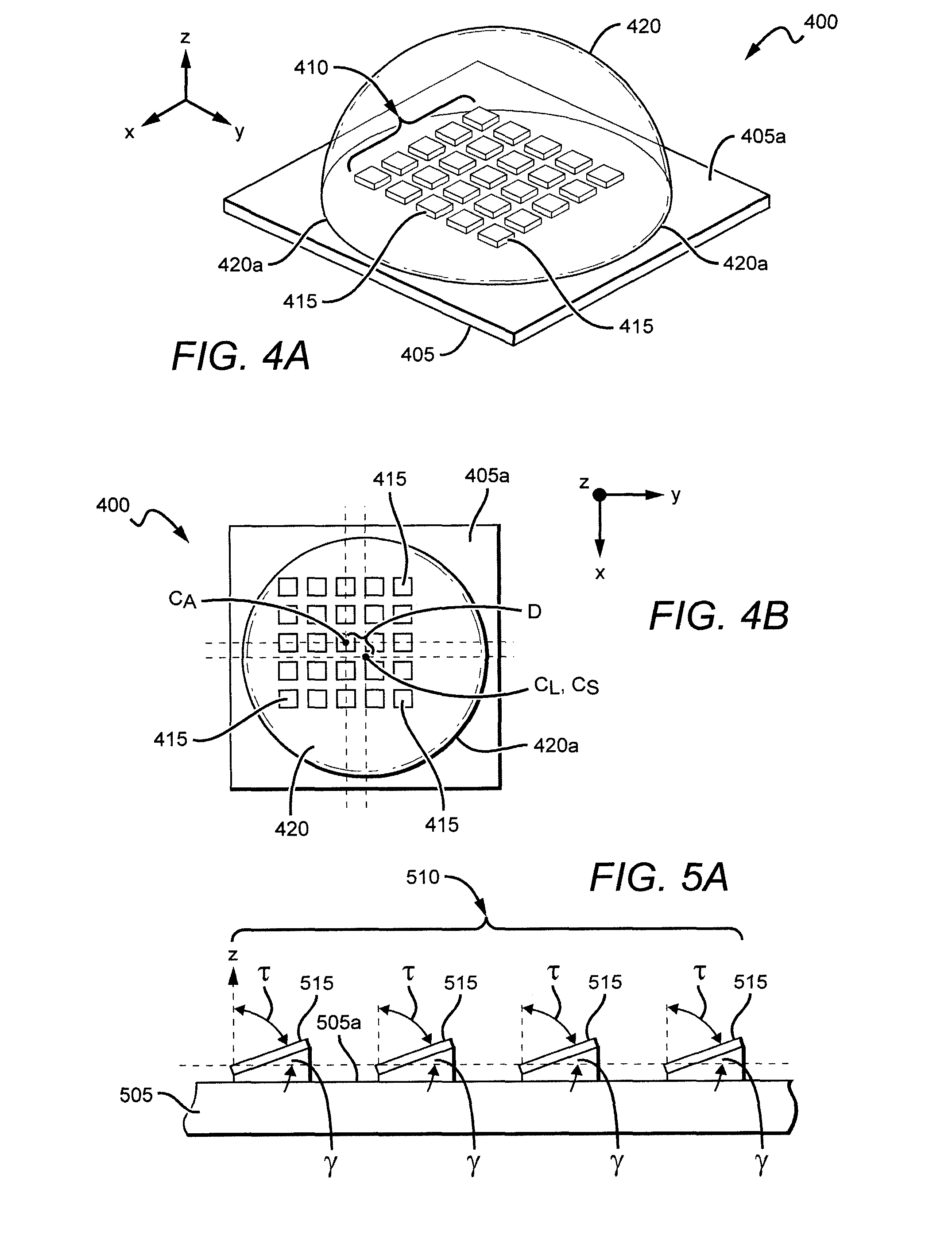
[0121]In this example, the center CA of a (2×2) chip array 1410 is offset as a unit with respect to the center CL of a single overlying lens 1420. The geometry of the array 1410 is shown in FIG. 14A. The offset D between the center CA of the LED chip array 1410 and the center CL of the lens 1420 (lens base 1420a) is varied and the resulting flux profile is obtained (FIG. 14B).
[0122]Referring to the data shown in FIG. 14B, a 0.3 mm offset between the center CA of the LED chip array 1410 and the center CL of the lens 1420 yields approximately a 10 degree shift in the position of the emission peak. A 0.6 mm offset between the center of the LED chip array and the center of the lens yields approximately a 20 degree shift in emission peak position.
[0123]In summary, the peak emission characteristics of the LED components described in the present patent document may be shifted away from the perpendicular centerline and in some cases otherwise modified for applications where a shifted, nonun...
PUM
 Abstract
Description
Claims
Application Information
 - R&D Engineer
- R&D Manager
- IP Professional
- Industry Leading Data Capabilities
- Powerful AI technology
- Patent DNA Extraction
Browse by: Latest US Patents, China's latest patents, Technical Efficacy Thesaurus, Application Domain, Technology Topic.
© 2024 PatSnap. All rights reserved.Legal|Privacy policy|Modern Slavery Act Transparency Statement|Sitemap