Display device and driving method of the same

a technology of a display device and a driving method, which is applied in the direction of electric digital data processing, instruments, computing, etc., can solve the problems of difficult to implement a large-sized or high-precision display, difficulty in controlling amoled displays, and high cost, so as to reduce or prevent the appearance of gray spots of display images, reduce or remove crosstalk phenomena, and clear image quality

Active Publication Date: 2014-05-01
SAMSUNG DISPLAY CO LTD
View PDF5 Cites 54 Cited by
  • Summary
  • Abstract
  • Description
  • Claims
  • Application Information

AI Technical Summary

Benefits of technology

[0014]Embodiments of the present invention have been made in an effort to provide a display device having features of implementing more accurate gray level expression and improved image quality in accordance with data signals by compensating for gray spots caused by variations in threshold voltages of driving transistors of pixels and by removing (or reducing) a crosstalk phenomenon from occurring when using a common initialization voltage.
[0015]Embodiments of the present invention have been made in an effort to provide a method of driving a display device capable of compensating for gray spots to implement high-quality display images by controlling the supply of an initialization (or initializing) voltage to pixels displaying each color of red, green, and blue (RGB) and capable of reducing a time required for compensating for variations (or deviations) in threshold voltages of the driving transistors of pixels displaying each color.
[0038]In the display device according to the exemplary embodiments of the present invention, it is possible to reduce or prevent the appearance of gray spots of a display image due to a deviation of threshold voltage of a driving transistor of a pixel included in a display panel device and to reduce or remove a crosstalk phenomenon through a supply control of initialization voltage to implement high-quality and clear image quality.
[0039]Further, it is possible to compensate for gray spots by controlling the supply of initialization voltage for a display image of a pixel displaying each color of red, green, and blue and to reduce a time required for compensation of variations in the threshold voltages of the driving transistors of a pixel displaying each color for each color pixel. Accordingly, it is possible to provide a stable driving method improving image quality of a display device because a high-speed driving method using a separate frame memory or sub frame is not required for the compensation of the gray spots.

Problems solved by technology

The passive matrix type OLED display has a simple structure and is relatively inexpensive, but it is difficult to implement a large-sized or high-precision panel.
On the other hand, the active matrix type OLED display may implement the large-sized or high-precision panel, but controlling AMOLED displays is technically difficult and the costs are relatively high.
In addition, the differences may occur due to deterioration of the driving transistor as the organic light emitting diode display is used over time.
Although the same data voltage is applied to each pixel circuit, the output emission degrees (e.g., brightnesses or gray levels) of the pixels vary due to non-uniformities in the threshold voltage characteristics of the driving transistors.
Accordingly, an accurate gray level is not expressed according to a data signal and a spot occurs, and, as a result, the quality of the display is deteriorated.
Technology for correcting for image degradation through the compensation of threshold voltage variation of the driving transistors has been developed, but recently, as display panels have grown in size and thus the display panel is driven at a higher speed, there are problems in that a compensation time is limited (e.g., the time available for compensation is short) and gray spots of the display panel may proliferate.

Method used


Image

  • Display device and driving method of the same
  • Display device and driving method of the same
  • Display device and driving method of the same

Examples


Embodiment Construction

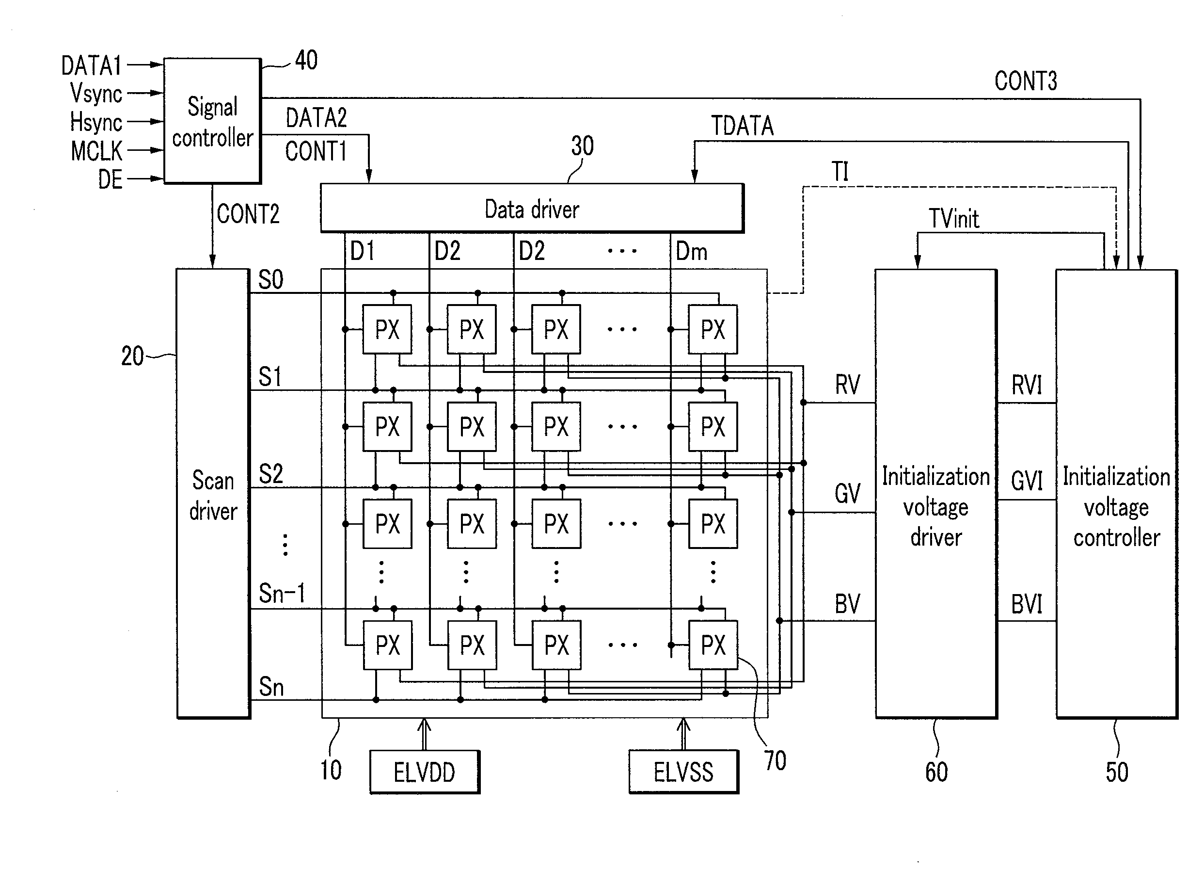
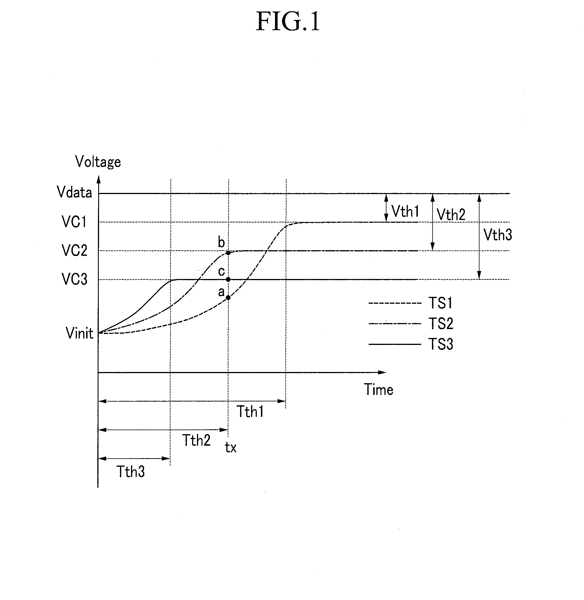
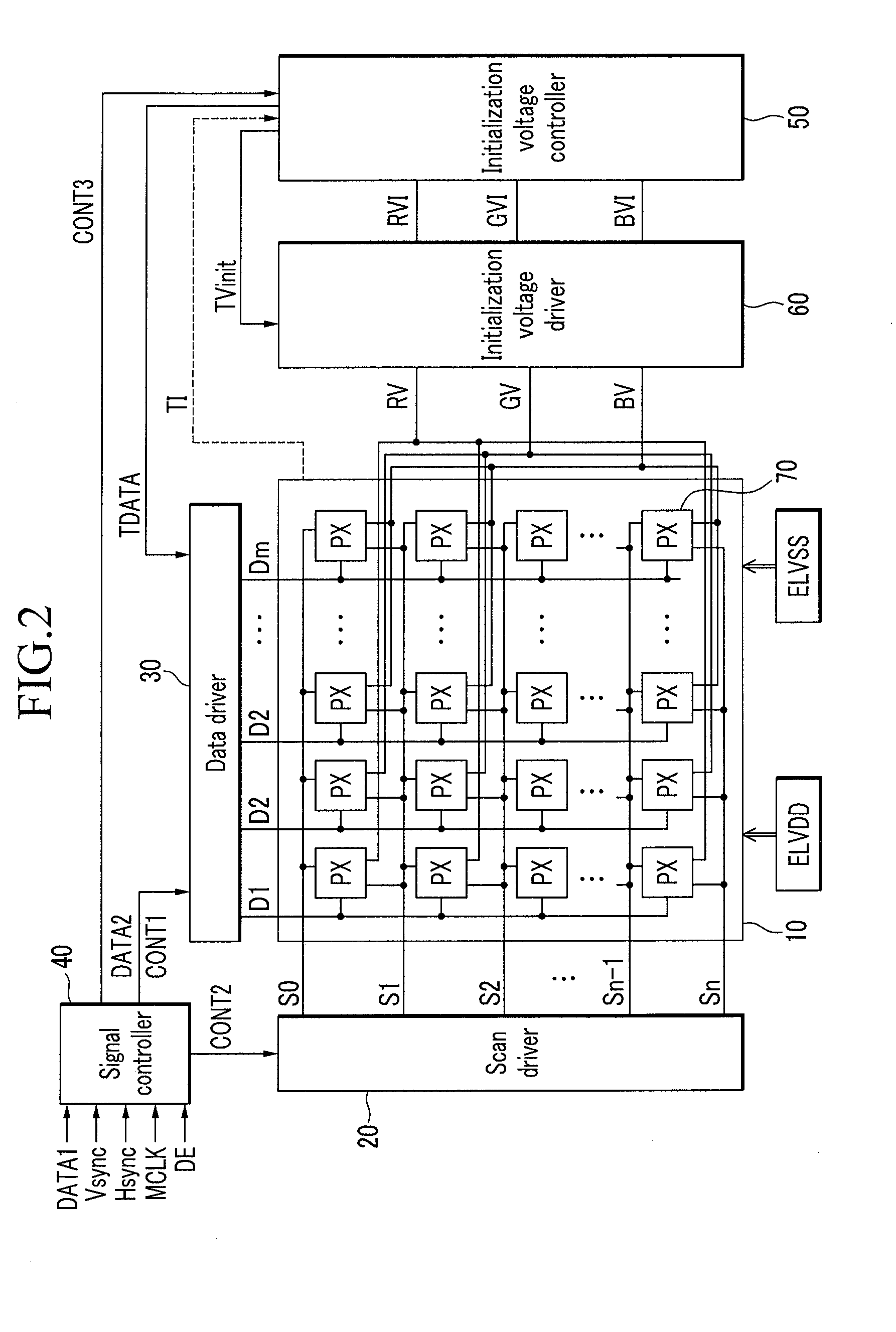
[0048]Embodiments of the present invention will be described more fully hereinafter with reference to the accompanying drawings, in which exemplary embodiments of the invention are shown. As those skilled in the art would realize, the described embodiments may be modified in various different ways, all without departing from the spirit or scope of the present invention.

[0049]The drawings and description are to be regarded as illustrative in nature and not restrictive. Like reference numerals designate like elements throughout the specification.

[0050]Throughout this specification and the claims that follow, when an element is described as being “coupled” to another element, the element may be “directly coupled” to the other element or “electrically coupled” to the other element through a third element. Further, unless explicitly described to the contrary, the word “comprise” and variations such as “comprises” or “comprising” will be understood to imply the inclusion of stated element...


PUM


Abstract

A display device includes: a display panel including scan lines, data lines, and color pixels located at crossing regions of the scan lines and the data lines, each of the color pixels including a driving transistor, the color pixels including first color pixels, second color pixels, and third color pixels; a scan driver configured to transfer a scan signal; a data driver configured to transfer an image data signal; an initialization voltage controller configured to set different initialization voltages for each pixel during each frame according to a threshold voltage deviation for the driving transistor of each pixel and calculate the initialization voltages including first, second, and third initialization voltages corresponding to the plurality of color pixels; an initialization voltage driver configured to apply the calculated first, second, and third initialization voltages; and a signal controller configured to generate and transfer a control signal and the image data signals.

Description

CROSS-REFERENCE TO RELATED APPLICATION[0001]This application claims priority to and the benefit of Korean Patent Application No. 10-2012-0119735 filed in the Korean Intellectual Property Office on Oct. 26, 2012, the entire disclosure of which is incorporated herein by reference.BACKGROUND[0002](a) Field[0003]Embodiments of the present invention relate to a display device and a driving method thereof.[0004](b) Description of the Related Art[0005]An organic light emitting diode display, which is a type of flat panel display apparatus, displays an image by using an organic light emitting diode which generates light by recombining electrons and holes. The organic light emitting diode display has a rapid response speed, low power consumption, and excellent emission efficiency, luminance, and viewing angles, and thus has received much attention.[0006]Generally, organic light emitting diode displays are classified into passive matrix organic light emitting diode displays (PMOLEDs) and acti...

Claims


Application Information

Patent Timeline
Patent Type & Authority Applications(United States)
IPC IPC(8): G09G5/02
CPCG09G5/02G09G3/3233G09G2300/0819G09G2300/0842G09G2300/0861G09G2310/0251G09G2320/0238G09G2320/0271G09G2320/0295G09G2360/145G09G3/30G09G3/3291
Inventor JUN, BYUNG-GEUNKIM, MIN-CHEOLKIM, IN-HWAN
Owner SAMSUNG DISPLAY CO LTD
Why Eureka
Try Eureka