Offset integrated circuit packaging interconnects

Active Publication Date: 2014-05-22
NVIDIA CORP
View PDF9 Cites 4 Cited by
  • Summary
  • Abstract
  • Description
  • Claims
  • Application Information

AI Technical Summary

Benefits of technology

This patent is about a way to make solder bump structures more durable and less prone to failure. By shifting the application of certain stresses to different temperatures, the method makes the structures warm and ductile, which reduces the likelihood of failure. This technique is useful for improving the reliability and durability of electronic components.

Problems solved by technology

Consequently, IC packaging techniques have encountered challenges for providing packaging which supports the requisite number of electrical connections.
Upon cooling, a CTE mismatch between the die and the substrate may cause shear and / or tensile stresses on the solder bump structures which attach the die to the substrate.
Consequently, repeatedly cycling the IC package from an operating temperature to a non-operating temperature may result in failure of the solder bump structures.

Method used


Image

  • Offset integrated circuit packaging interconnects
  • Offset integrated circuit packaging interconnects
  • Offset integrated circuit packaging interconnects

Examples


Embodiment Construction

[0017]In the following description, numerous specific details are set forth to provide a more thorough understanding of embodiments of the present invention. However, it will be apparent to one of skill in the art that embodiments of the present invention may be practiced without one or more of these specific details.

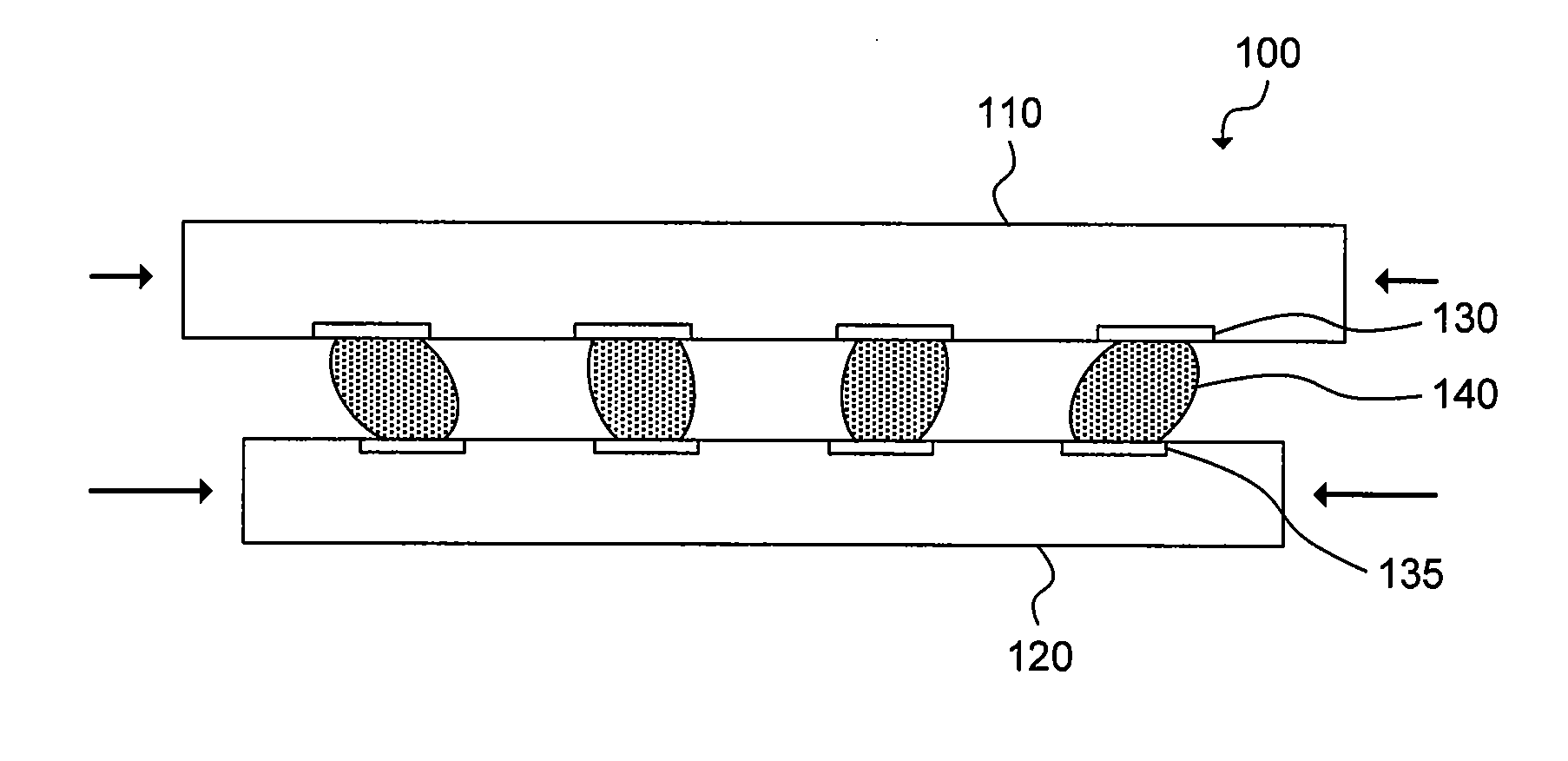
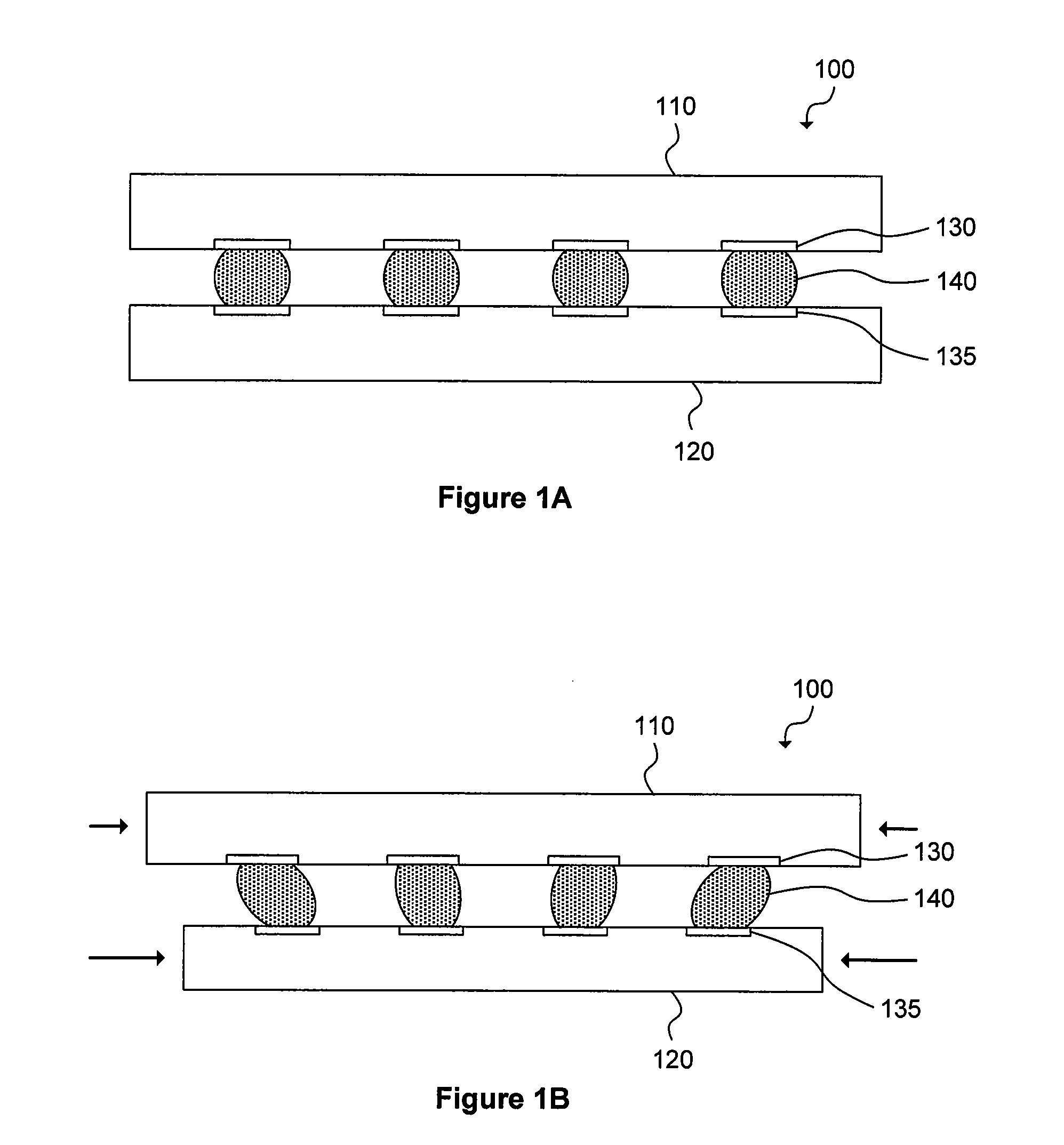
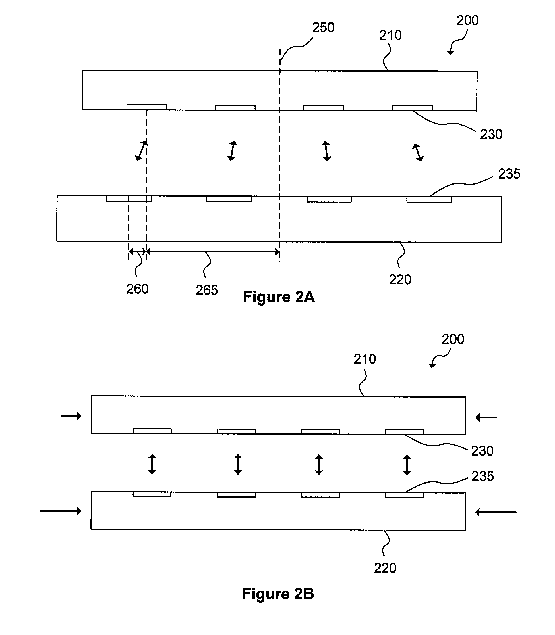
[0018]FIGS. 1A and 1B illustrate schematic views of an integrated circuit (IC) package 100 having a conventional configuration. The conventional IC package 100 includes a die 110, a conventional substrate 120, a plurality of die interconnects 130, a plurality of substrate interconnects 135, and a plurality of solder balls 140. The plurality of solder balls 140 mechanically and electrically couple the die 110 to the conventional substrate 120 and provide electrical connections between the die interconnects 130 and the substrate interconnects 135.

[0019]FIG. 1A illustrates the conventional IC package 100 when heated to an operating temperature. In conventional “flip chip” ...


PUM


Abstract

One embodiment of the present invention sets forth an integrated circuit package including a substrate, an integrated circuit die, and a plurality of solder bump structures. The substrate includes a first plurality of interconnects disposed on a first surface of the substrate. The integrated circuit die includes a second plurality of interconnects disposed on a first surface of the integrated circuit die. The plurality of solder bump structures couple the first plurality of interconnects to the second plurality of interconnects. The first plurality of interconnects are configured to be substantially aligned with the second plurality of interconnects when the integrated circuit package is at a first temperature within a range of about 0° C. to about −100° C. The first plurality of interconnects are configured to be offset from the second plurality of interconnects when the integrated circuit package is at a temperature above the first temperature.

Description

BACKGROUND OF THE INVENTION[0001]1. Field of the Invention[0002]Embodiments of the present invention generally relates to integrated circuit packaging interconnects.[0003]2. Description of the Related Art[0004]Integrated circuit (IC) fabrication is a multi-step sequence which includes processes such as patterning, deposition, etching, and metallization. Typically, in the final processing steps, the resulting IC die are separated and packaged. IC packaging serves several purposes, including providing an electrical interface with the die, providing a thermal medium through which heat may be removed from the die, and / or providing mechanical protection for the die during subsequent usage and handling.[0005]One type of IC packaging technique is referred to as “flip chip” packaging. In flip chip packaging, after the metallization process is complete, solder bump structures (e.g., solder balls, pads, etc.) are deposited on the die, and the die is separated from the wafer (e.g., via dicing,...

Claims


Application Information

Patent Timeline
IPC IPC(8): H01L23/488H01L21/48
CPCH01L24/16H01L23/49838H01L2924/07802H01L2224/16105H01L2924/351H01L2224/16108H01L2924/381H01L2224/81194H01L2924/00H01L21/4853H01L23/488
Inventor ZHANG, LEILEIBOKHAREY, ZUHAIR
Owner NVIDIA CORP
Why Eureka
Try Eureka